How to make printed circuit boards: a tour of the factory Tehnoteh
Today we will perform in a bit unusual role for ourselves, we will not talk about gadgets, but about the technologies that stand behind them. A month ago we were in Kazan, where we met with the guys from the Navigator campus . At the same time, they visited a closely located (well, relatively close) factory for the production of printed circuit boards - Technotech . This post is an attempt to figure out how to produce those same printed circuit boards.
So, how do we make circuit boards for our favorite gadgets?
The factory knows how to make boards from the beginning to the end - designing boards according to your TZ, making fiberglass, manufacturing single-sided and double-sided printed circuit boards, manufacturing multi-layer printed circuit boards, marking, checking, manual and automatic assembly and soldering of boards.
For starters, I'll show you how double-sided boards are made. Their technical process is no different from the production of single-sided printed circuit boards, except that in the manufacture of OPP do not perform operations on the second side.
About board making methods
In general, all methods for the manufacture of printed circuit boards can be divided into two broad categories: additive (from the Latin additio — addition) and subtractive (from the Latin subtratio — attention). An example of a subtractive technology is the well-known LUT (Laser-iron technology) and its variations. In the process of creating a printed circuit board using this technology, we protect future tracks on a sheet of fiberglass laminate with toner from a laser printer, and then bleed everything unnecessary in ferric chloride.
In additive methods, conductive paths, on the contrary, are applied to the surface of the dielectric in one way or another.
Semiadditive methods (sometimes they are also called combined.) Are a cross between the classical additive and subtractive methods. In the process of producing PP according to this method, a part of the conductive coating can be etched (sometimes almost immediately after application), but as a rule it happens faster / easier / cheaper than in subtractive methods. In most cases, this is due to the fact that most of the thickness of the tracks is increased by electroplating or chemical methods, and the layer that is etched is thin, and serves only as a conductive coating for galvanic deposition.
I will show exactly the combined method.
')
Production of double-layer printed circuit boards using a combined positive method (semi-additive method)
Fiberglass fabrication
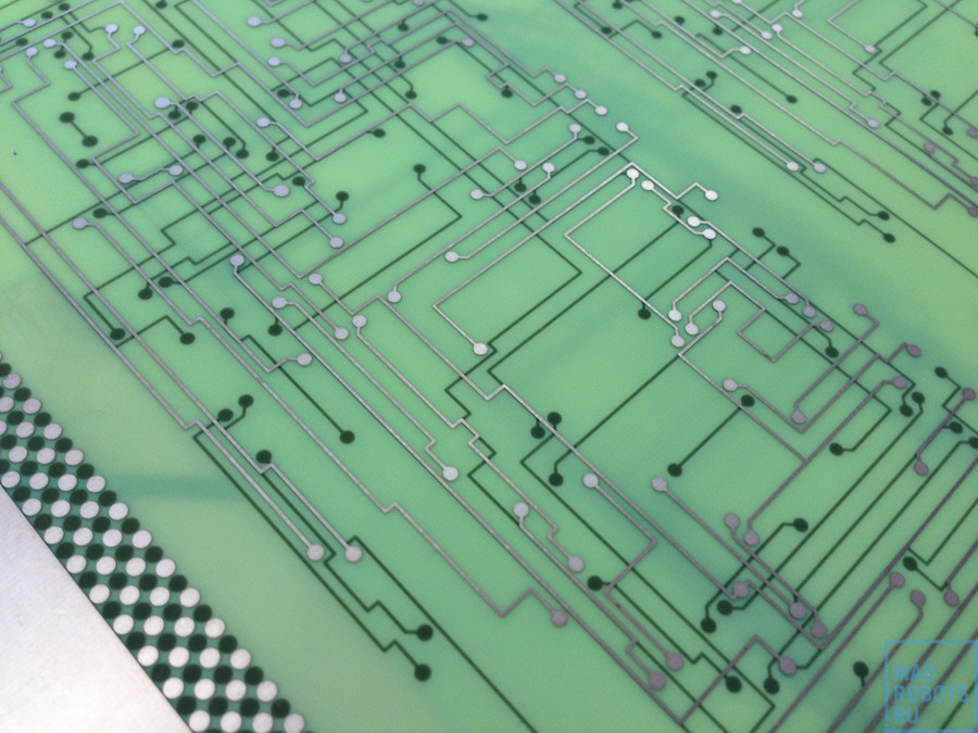
The process begins with the manufacture of foil fiberglass. Glass fiber is a material consisting of thin sheets of fiberglass (they look like a dense shiny fabric), impregnated with epoxy resin and pressed into a stack of sheets.
Fiberglass cloths themselves are not too simple either - they are wicker (like ordinary fabric in your shirt) thin-thin strands of ordinary glass. They are so thin that they can easily bend in any direction. It looks like this:

You can see the orientation of the fibers on the long-suffering picture from Wikipedia:
In the center of the board, the light areas are fibers perpendicular to the shear, the areas are slightly darker - parallel.
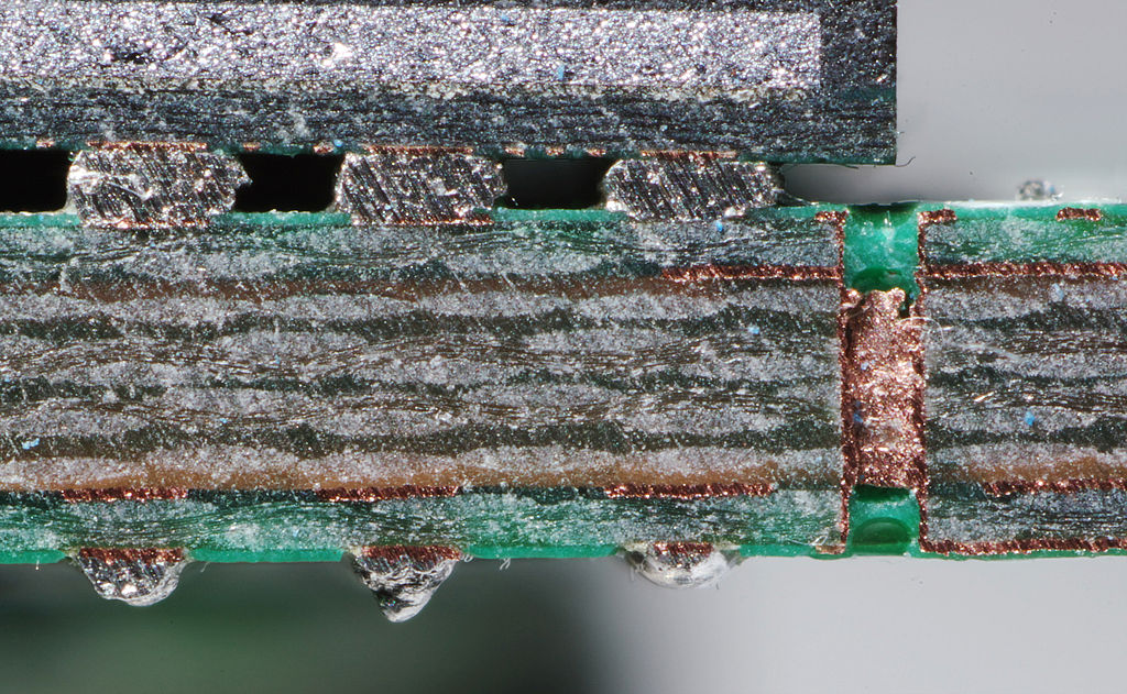
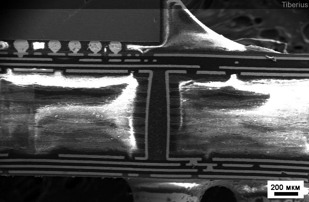
Or, for example, on micrographs of tiberius , as I recall from this article:
So, let's begin.
Fiberglass cloth is supplied to production here in such reels:
It is already impregnated with partially cured epoxy resin - such a material is called a prepreg , from English pre- im preg nated - previously impregnated. Since the resin is already partially cured, it is no longer as sticky as it is in the liquid state - sheets can be picked up by hands, without being afraid to get dirty in the resin. The resin will become liquid only when the foil is heated, and then only for a few minutes before solidifying completely.
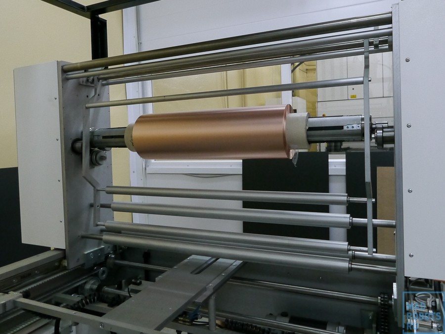
The required number of layers together with copper foil is collected on this machine:
But the foil roll itself.
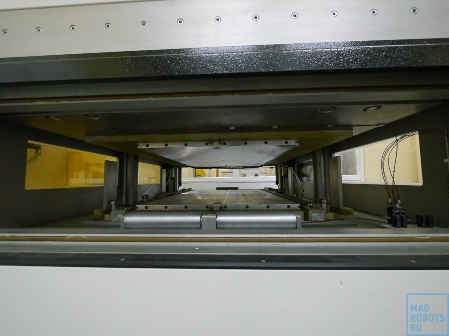
Next, the canvas is cut into pieces and enters a press with a height of two human height:

On the photo is Vladimir Potapenko, production manager.
Interestingly, the heating technology was implemented during pressing: it was not the parts of the press that heated, but the foil itself. A current is supplied to both sides of the sheet, which, due to the resistance of the foil, heats the sheet of the future fiberglass. Pressing takes place under severely reduced pressure, to eliminate the appearance of air bubbles inside the PCB.
When pressing, due to heat and pressure, the resin softens, fills the voids and after polymerization a single sheet is obtained.
Here is this:
It is cut into blanks for boards with a special machine:
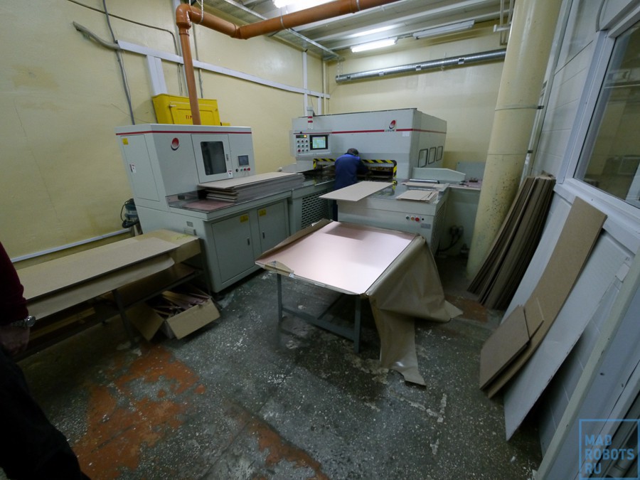
Technotech uses two types of blanks: 305x450 - a small group blank, 457x610 - a large blank
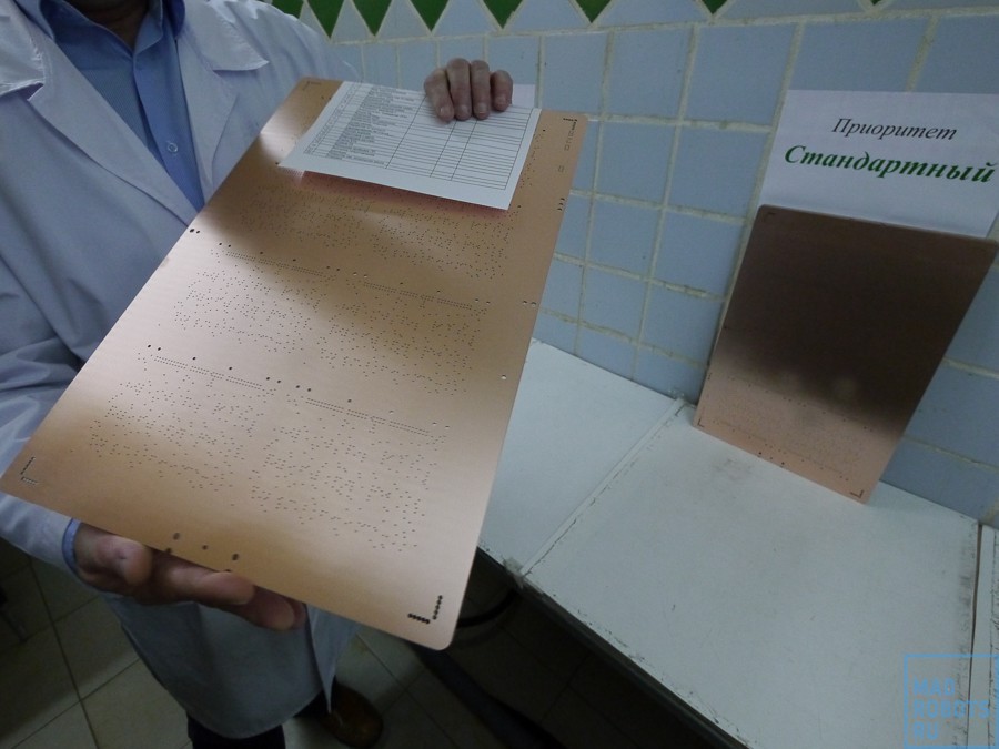
After that, for each set of blanks a route map is printed, and the journey begins ...
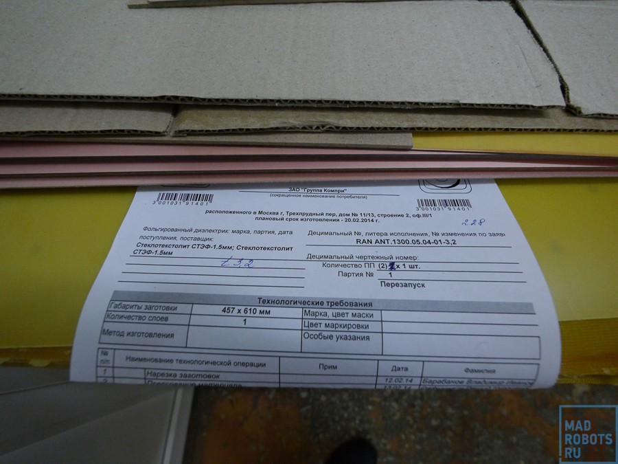
The route map is such a piece of paper with a list of operations, information about the board and a bar code. To control the execution of operations, 1C 8 is used, which contains all the information about orders, technical process, and so on. After the next production stage is completed, the barcode is scanned on the route list and entered into the database.
Drill blanks
The first stage of production of single-layer and two-layer printed circuit boards - drilling holes. With multilayer boards everything is more complicated, and I will tell about it later. Billets with route sheets arrive at the drill site:
From blanks going package for drilling. It consists of a substrate (material such as plywood), from one to three identical pieces of printed circuit boards and aluminum foil. Foil is needed to determine if the drill touches the workpiece surface - this is how the machine determines the breakage of the drill. Even with each capture of the drill, he controls its length and sharpening with a laser.
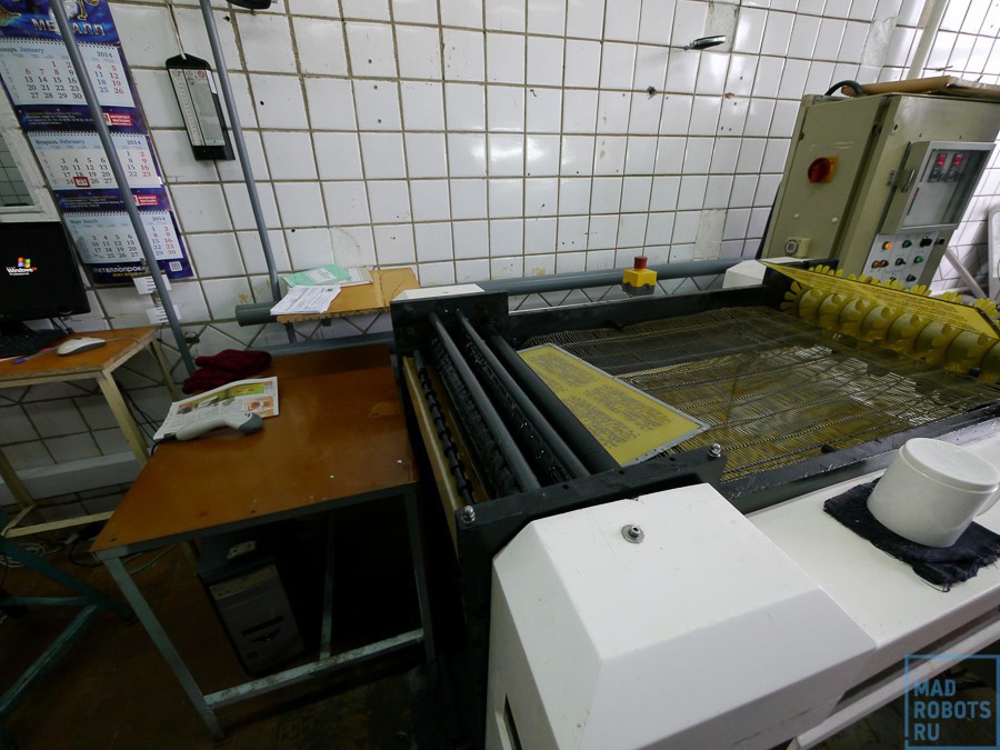
After the package is assembled, it is laid in this machine:
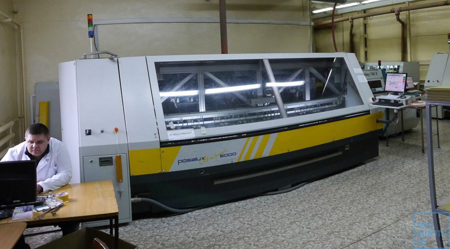
It is so long that I had to stitch this picture out of several frames. This is a Swiss machine company Posalux, the exact model, unfortunately I do not know. According to the characteristics it is close to this . He eatsthree -time three -phase 400V power supply, and consumes 20 kW during operation. Machine weight about 8 tons. It can simultaneously process four packages for different programs, which gives a total of 12 boards per cycle (of course, all the blanks in the same package will be drilled the same way). Drilling cycle - from 5 minutes to several hours, depending on the complexity and number of holes. The average time is about 20 minutes. In total, there are three such machines at tech-tech.
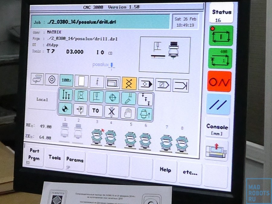
The program is developed separately, and loaded over the network. All the operator needs to do is scan the barcode of the lot and lay a package of blanks inside. Capacity tool shop: 6000 drills or cutters.
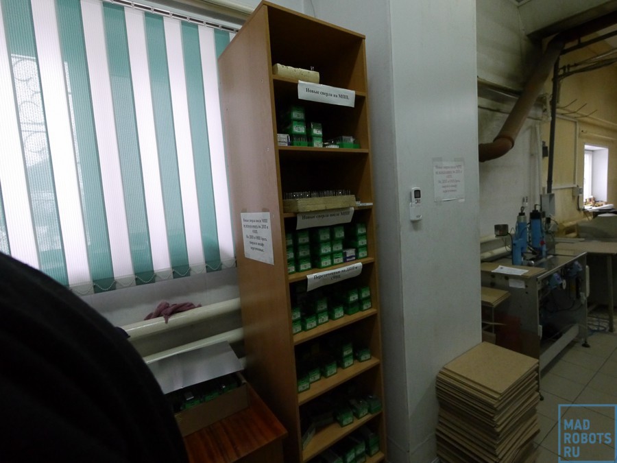
Nearby there is a large cabinet with drills, but the operator does not need to monitor the sharpening of each drill and change it - the machine always knows the degree of wear of the drills - it records to itself how many holes were drilled by each drill. When the resource is exhausted, the drill itself changes to a new one; the old drill will be left unloaded from the container and sent for re-grinding.

Here is the interior of the machine:

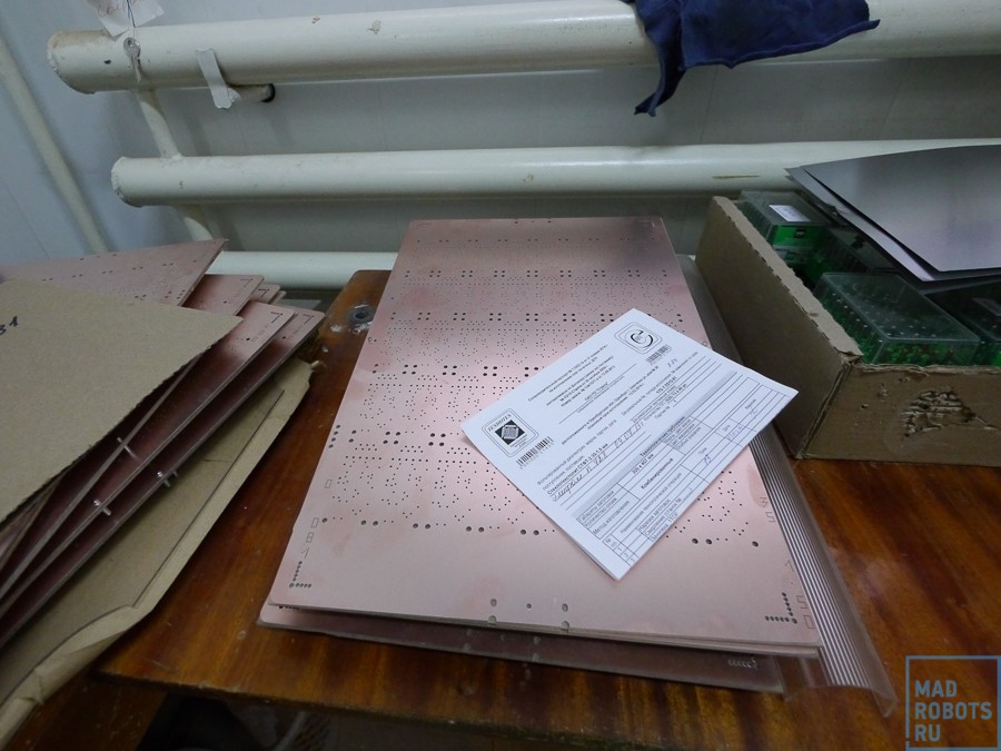
After drilling in the route list and the base is a mark, and the fee is senton stage to the next stage.
Cleaning, activation of blanks and chemical copper plating.
Although the machine uses its “vacuum cleaner” during and after drilling, the surface of the board and the holes still need to be cleaned of dirt and prepared for the next process operation. For a start, the board is simply cleaned in the washing solution with mechanical abrasives.
The inscriptions, from left to right, are: “Stripping chamber with brushes up / down”, “Washing chamber”, “Neutral zone”.
The fee becomes clean and shiny:
After this, the surface activation process is carried out in a similar installation.A serial number is entered for each surface. Surface activation is the preparation for copper deposition on the inner surface of the holes to create vias between the layers of the board. Copper can not settle on the unprepared surface, so the board is treated with special catalysts based on palladium. Palladium, unlike copper, is easily deposited on any surface, and further serves as crystallization centers for copper. Activation setting:

After that, successively passing several baths in another similar installation, the billet acquires a thin (less than micron) layer of copper in the holes.

Further, this layer of electroplating increases to 3-5 microns - this improves the resistance of the layer to oxidation and damage.
Application and exposure of photoresist, removal of undelayed areas.
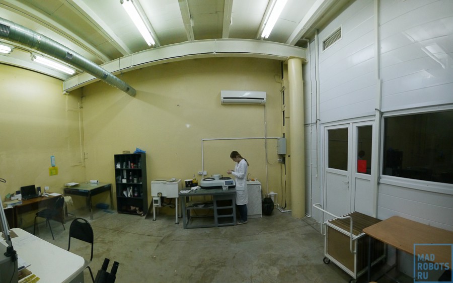
Then the board goes to the site of photoresist application. We were not allowed there, because it is closed, and in general, there is a clean room, so we confine ourselves to photographs through glass. I saw something similar in Half-Life (I’m talking about pipes coming down from the ceiling):
Actually, here is the green film on the drum - this is the photoresist.
Further, from left to right (in the first photo): two settings for applying photoresist, then automatic and manual frames for illumination using previously prepared photomasks. In the automatic frame there is a control that takes into account the tolerance for alignment with reference points and holes. In the manual frame, the mask and the board are combined hands. Silkscreen and solder mask are displayed on the same frames. Next is the installation of developing and washing the boards, but since we did not get there, I don’t have photos of this part. But there is nothing interesting about the same conveyor as in the “activation”, where the workpiece passes successively several baths with different solutions.
And in the foreground is a huge printer that prints these same photo masks:
Here is a board with printed, exposed, and developed:
Please note that the photoresist is applied on the places where copper will not be in the future - the mask is negative and not positive, as in LUT or home photoresist. This is because in the future the build-up will take place at the locations of future tracks.
This is also a positive mask:

All these operations occur with nonactinic lighting, the spectrum of which is chosen in such a way as not to have an effect on the photoresist and to give maximum illumination for the work of a person in a given room.
I love ads, the meaning of which I do not understand:
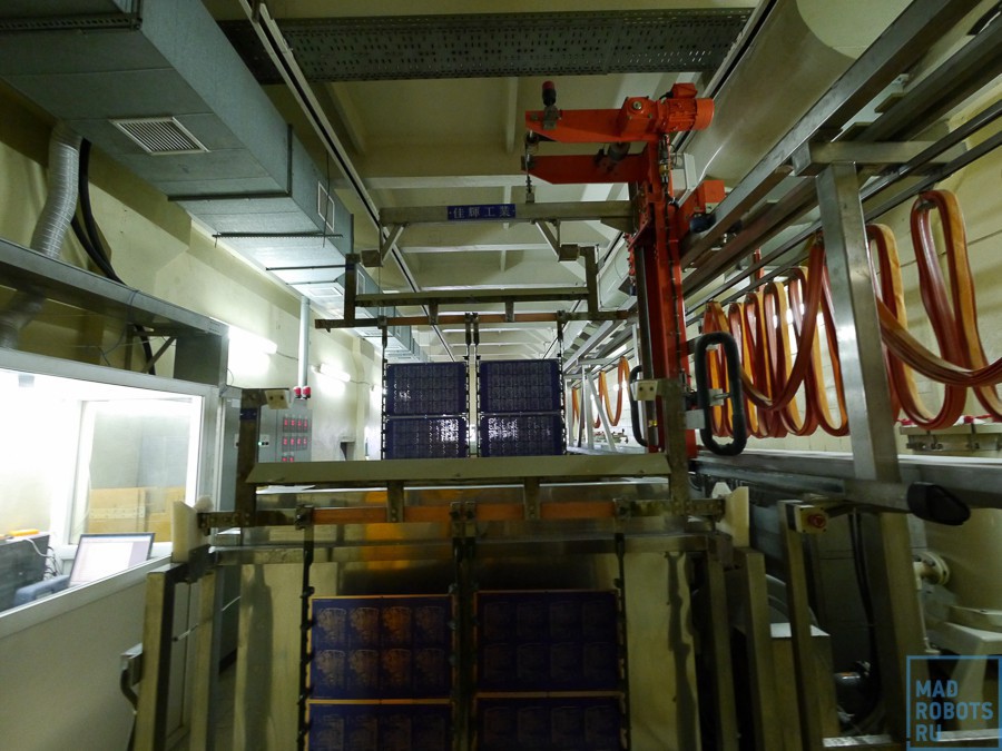
Galvanic plating
Now came through her majesty - electroplating metallization. In fact, it was already carried out at the last stage, when a thin layer of chemical copper was growing. But now the layer will be increased even more - from 3 microns to 25. This is the layer that conducts the main current in the vias. This is done in such baths:
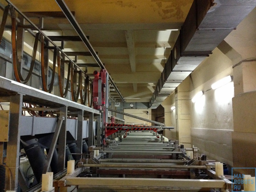
In which complex electrolyte compositions circulate:
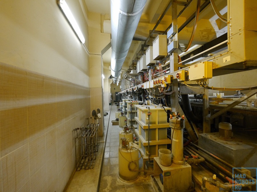
And a special robot, obeying a pledged program, drags boards from one bath to another:
One cycle of copper plating takes 1 hour and 40 minutes. 4 blanks can be processed in one pallet, but there can be several such pallet in the bath.
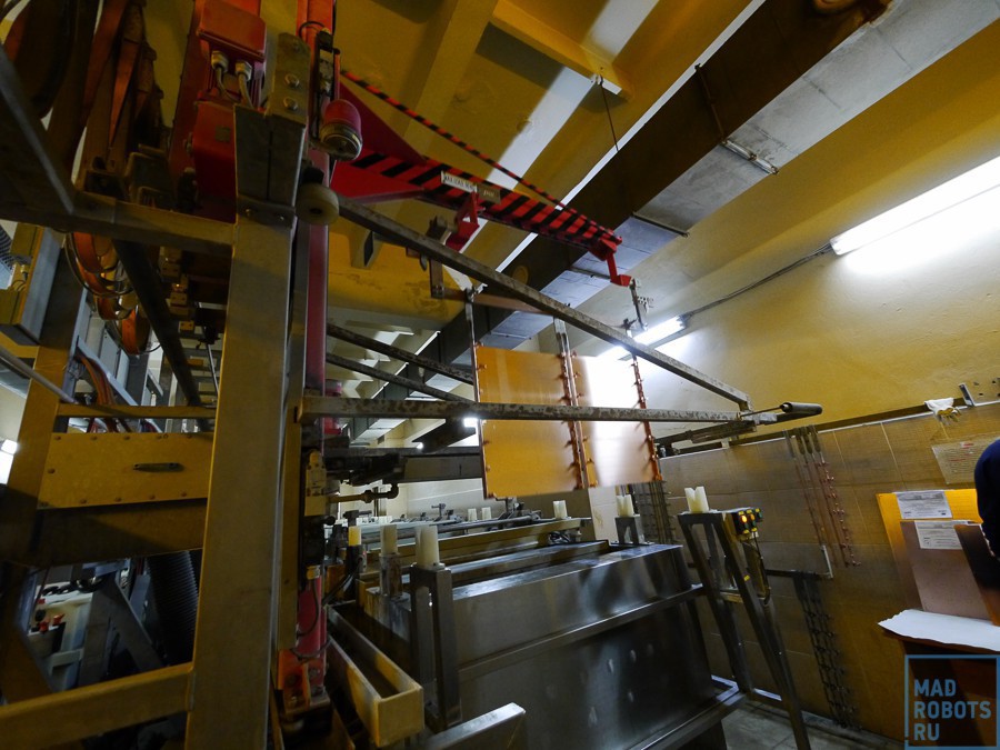
Deposition of metal resist
The next operation is another galvanic metallization, only now the deposited material is not copper, and the PIC is lead-tin solder. And the coating itself, by analogy with a photoresist, is called a metal resist. Boards are installed in the frame:

This frame passes several electroplating baths already familiar to us:
And covered with a white layer of PIC. In the background you can see another board, not yet processed:

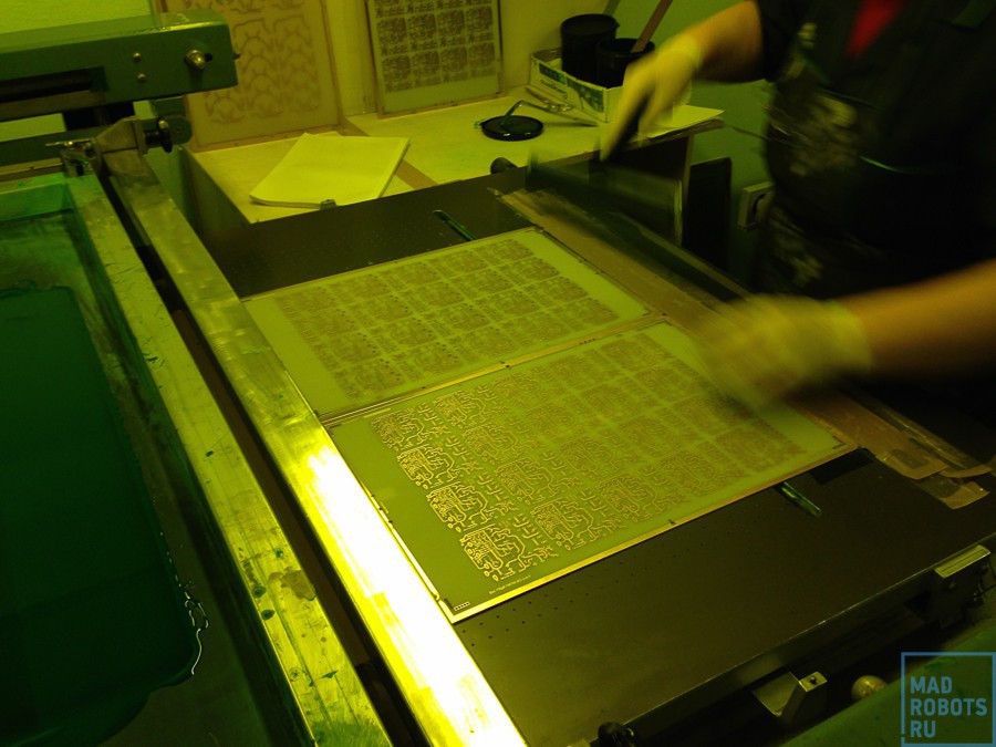
Removal of photoresist, etching of copper, removal of metalresist

Now the photoresist is washed off the boards, it has fulfilled its function. Now there are still metal-covered tracks on the still copper plate. At this installation etching occurs in a cunning solution, which etches copper, but does not touch the metal resist. As far as I remember, it consists of ammonium carbonate, ammonium chloride and ammonium hydroxide. After etching, the boards look like this:

The tracks on the board are a “sandwich” made from the bottom layer of copper and the top layer of the galvanic POS. Now, with another, even more tricky solution, another operation is carried out — the PIC layer is removed without affecting the copper layer.
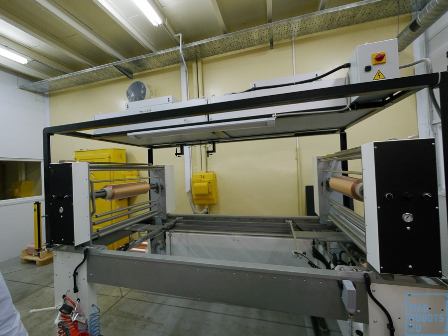
However, sometimes the PIC is not removed, but melted in special furnaces. Or the board undergoes hot-dip (HASL-process) - when it sinks into a large solder bath. First, it is coated with rosin flux:
And here it is installed in this machine:
He lowers the board in a bath with solder and immediately pulls it back. Air flows blow off excess solder, leaving only a thin layer on the board. The fee is obtained like this:
But in fact, the method is a bit “barbaric” and does not really affect the boards, especially multi-layered ones — when immersed in the solder melt, the board suffers a temperature shock, which does not work very well on the internal elements of multi-layer boards and thin single- and double-layer tracks.
It is much better to cover with immersion gold or silver. Here is very good information about immersion coatings, if anyone is interested.
We did not visit the site of immersion coatings, for a banal reason - it was closed, and the key was too lazy. It's a pity.
Electrotest
Then almost ready boards are sent for visual inspection and electrical test. Electric test is when the connections of all contact pads between themselves are checked, whether there are any breaks. It looks very funny - the machine holds the board and quickly pokes probes into it. You can watch the video of this process in my instagram (by the way, you can subscribe there). And in the form of a photo it looks like this:
That big car on the left is an electric test. And here are the probes themselves closer:

In the video, however, there was another machine - with 4 probes, and here there are 16. They are said to be much faster than all three old machines with four probes combined.
Application of solder mask and coating of contact pads
The next process is applying a solder mask. That is the greenest (well, most often greenish. In general, it comes in very different colors) the coating that we see on the surface of the boards. Prepared fees:
Mounted here in this machine:
Which through a thin mesh spreads semi-fluid mask on the surface of the board:
Video drawing, by the way, can also be viewed in instagram (and subscribe too :)
After that, the boards dry until the mask stops sticking and are exhibited in the same yellow room that we saw above. After that, the unexposed mask is washed away, exposing the contact patches:
Then they are covered with a finishing coating - hot-dip or immersion coating:

And put the label - silk screen. These are white (most often) letters that show where a connector is and what element stands here.
It can be applied using two technologies. In the first case, everything is the same as with the solder mask, only the color of the composition is different. It covers the entire surface of the board, then it is exposed, and the areas uncured by ultraviolet light are washed away. In the second case, it is applied by a special printer printing with a cunning epoxy composition:

It is cheaper and much faster. The military, by the way, does not favor this printer, and constantly indicate in the requirements for their cards that the marking is applied only with a photopolymer, which is very distressing to the chief process engineer.
Production of multi-layer printed circuit boards by the method of metallization of through holes:
All that I have described above concerns only one-sided and double-sided printed circuit boards (at the factory, by the way, no one calls them that way, everyone says OPP and DPP). Multilayer boards (WFP) are made on the same equipment, but with a slightly different technology.
Making cores
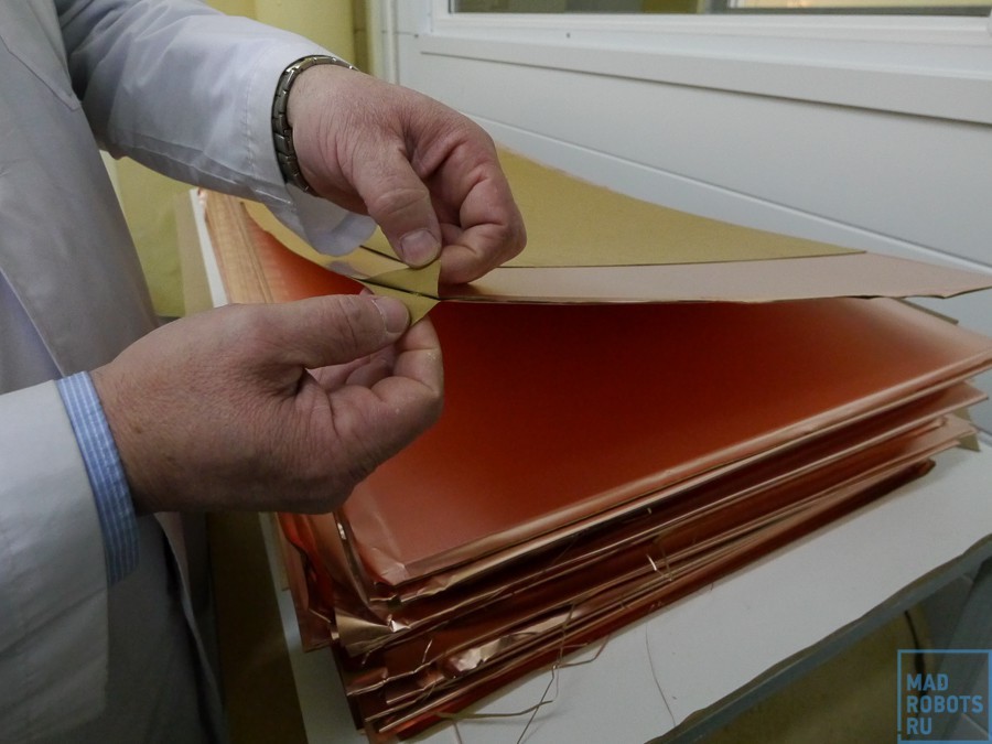
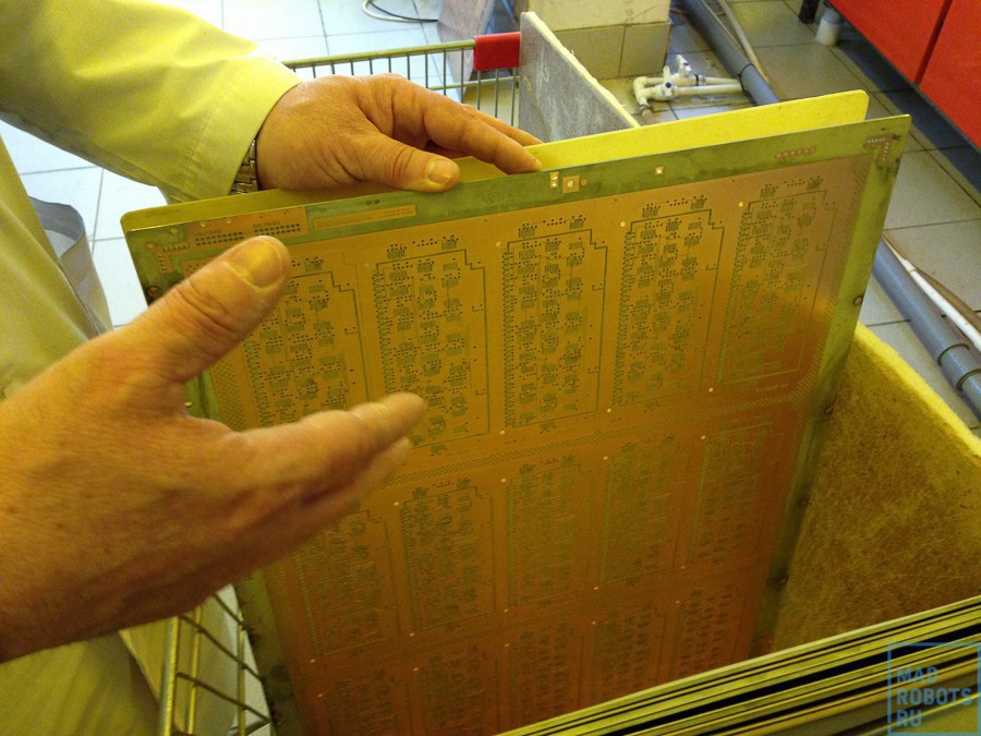
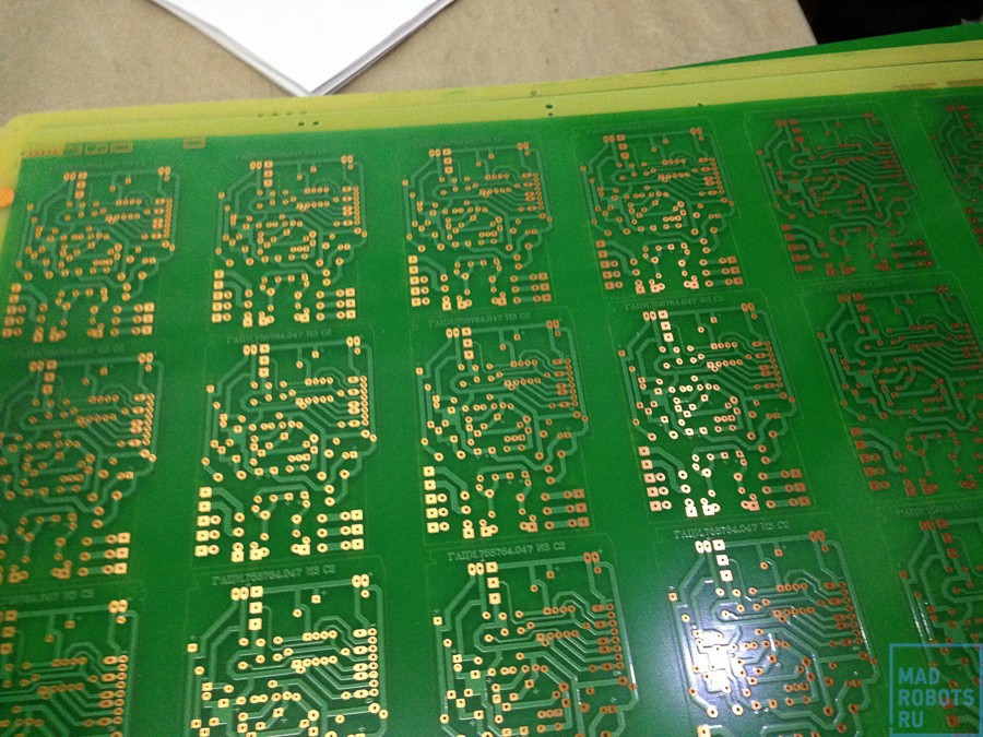
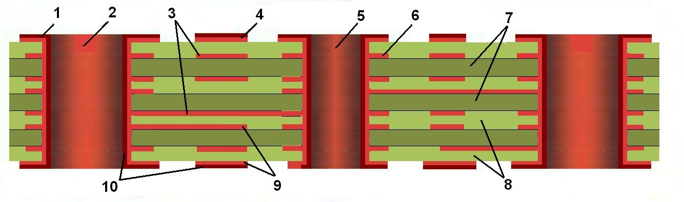
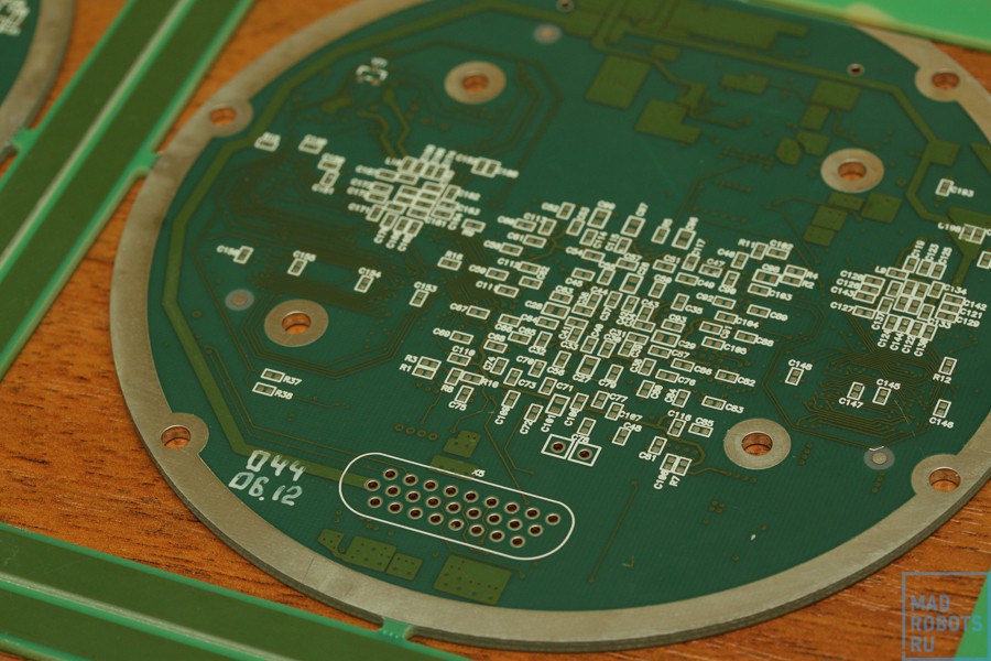
The core is the inner layer of a thin PCB with copper conductors on it. Such cores in the board can be from 1 (plus two sides - a three-layer board) to 20. One of the cores is called gold - this means that it is used as a reference layer - the layer along which all the others are exposed. The kernels look like this:

They are made in the same way as conventional boards, only the thickness of the fiberglass laminate is very small - usually 0.5 mm. The sheet is so thin, it can be bent like thick paper. A copper foil is applied to its surface, and then all the usual stages occur - application, exposure of photoresist and etching. The result of this are the following sheets:
After manufacturing, the tracks are checked for integrity on the machine, which compares the board pattern to the clearance with the photo mask. In addition, there is also a visual control. And really visual - people are sitting and looking at the blanks:

Sometimes one of the control stages makes a verdict about the poor quality of one of the blanks (black crosses):
This sheet of boards, in which the defect occurred, will be made completely anyway, but after cutting the defective board will go to the garbage. After all the layers have been manufactured and tested, it is the turn of the next technological operation.
Assembly of the cores in the package and pressing
This takes place in the hall called “Plot pressing”:

The cores for the board are laid out in this pile:
And next is a map of the location of the layers:

After that, the semi-automatic board pressing machine comes into play. Its semi-automaticity lies in the fact that the operator must, at her command, deliver the cores to it in a certain order.
Shifting them for insulation and bonding with prepreg sheets:

And then the magic begins. The machine captures and transfers sheets to the working field:
And then combines them along the reference holes relative to the gold layer.
Then the blank goes to a hot press, and after warming up and polymerization of the layers - to a cold one. After that we get the same sheet of fiberglass, which is no different from the blanks for double-layer printed circuit boards. But inside he has akind heart with several cores with formed tracks, which, however, are not connected to each other and are separated by insulating layers of polymerized prepreg. Then the process goes through the same stages that I described earlier. True, with a slight difference.
Drill blanks
When assembling an OPP and DPP package for drilling, it does not need to be centered, and it can be assembled with a certain tolerance - this is still the first technological operation, and everyone else will be guided by it. But when assembling a package of multilayer printed circuit boards, it is very important to bind to the inner layers - when drilling a hole must go through all the internal contacts of the cores, connecting them in ecstasy during metallization. Therefore, the package is going here on this machine:
This is an X-ray drilling machine, which sees through the textolite the internal metallic reference marks and, by their location, drills the basic holes, into which the fasteners are inserted to install the package into the drilling machine.

Metallization
Then everything is simple - billets are drilled, cleaned, activated and metallized. The metallization of the hole interconnects all the copper heels inside the circuit board:
Thus, completing the electronic circuit of the interior of the circuit board.
Check and grinding
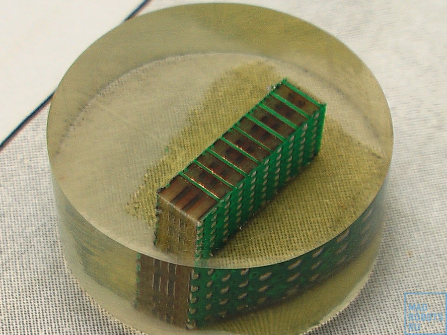
Further a piece is cut from each board, which is polished and examined with a microscope in order to make sure that all the holes turned out to be normal.
These pieces are called thin sections - transversely cut off parts of the printed circuit board, which allows you to evaluate the quality of the board as a whole and the thickness of the copper layer in the central layers and vias. In this case, under the thin section, they do not allow a separate payment, but the entire set of diameters of vias, specially made from the edge of the board, which are used in the order. The grout embedded in the transparent plastic looks like this:
Milling or scribing
Next, the boards that are on the group blank must be divided into several parts. This is done either on a milling machine:

Which frezoy cuts the desired path.Another option is scribing, this is when the outline of the board is not cut, but is incised with a round knife. It is faster and cheaper, but allows you to make only rectangular boards, without complex contours and internal cuts. Here is a scribed board:
And here is a milled one:
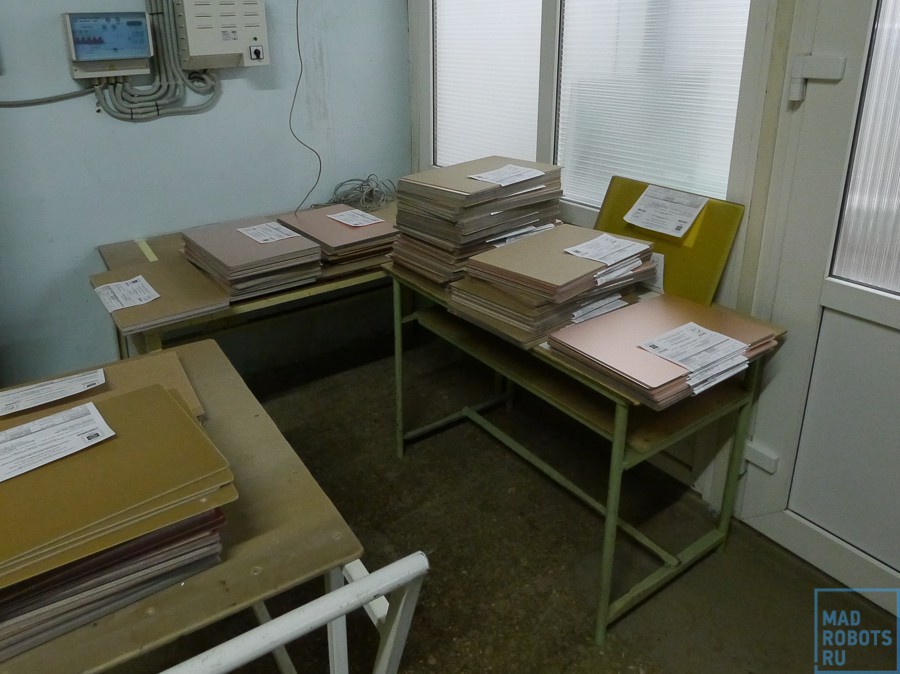
If only the production of boards was ordered, then this ends up - the boards are put in a pile: It turns
around with the same route list:

And it waits for sending.
And if assembly and sealing is needed, then there is still something interesting ahead.
Assembly
Then the board, if necessary, enters the assembly area, where the necessary components are soldered on it. If we are talking about manual assembly, then everything is clear, people are sitting (by the way, most of the women, when I went to them, my ears curled up from the tape song “God, what a man”):
And they collect, collect:

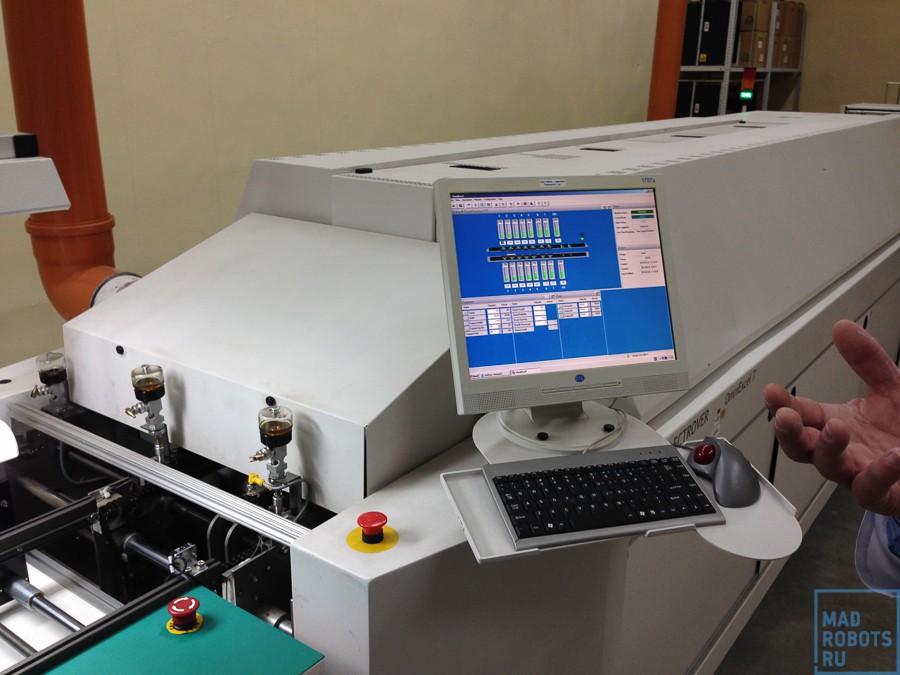
But if we talk about automatic assembly, then everything is much more interesting. It happens here on such a long 10-meter installation, which does everything - from applying solder paste to soldering on thermal profiles.
By the way, everything is serious. Even the mats are grounded there:

As I said, it all starts with the fact that the uncut sheet with printed circuit boards is installed with the metal template at the beginning of the machine. The solder paste is thickly smeared on the template, and the doctor blade passing from above leaves precisely measured quantities of paste in the cavities of the template.
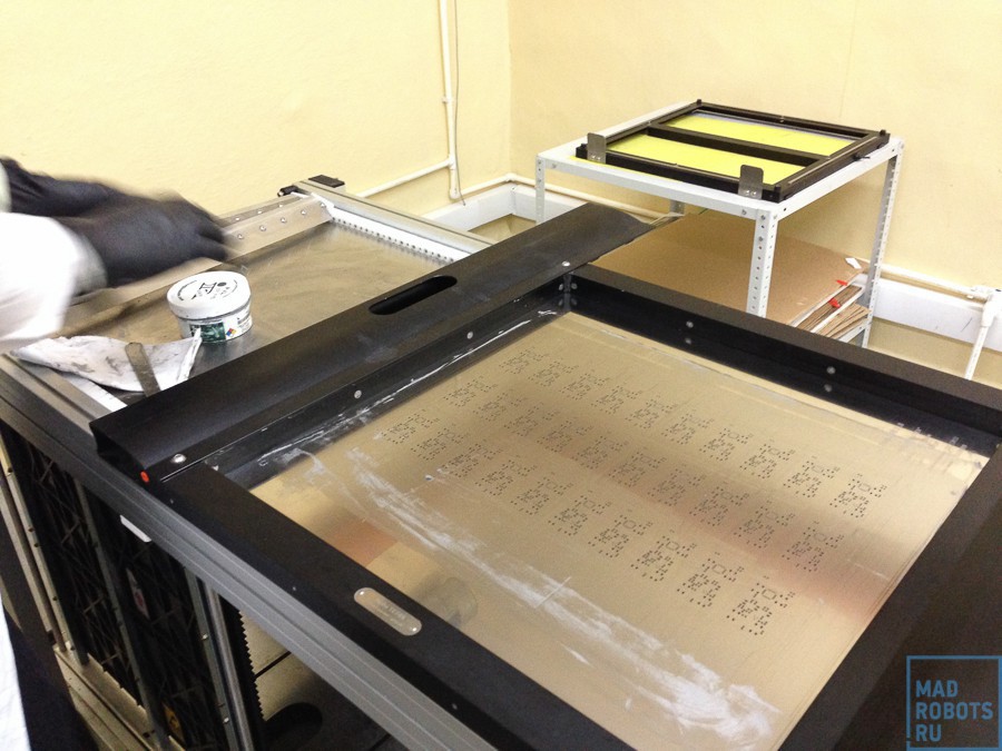
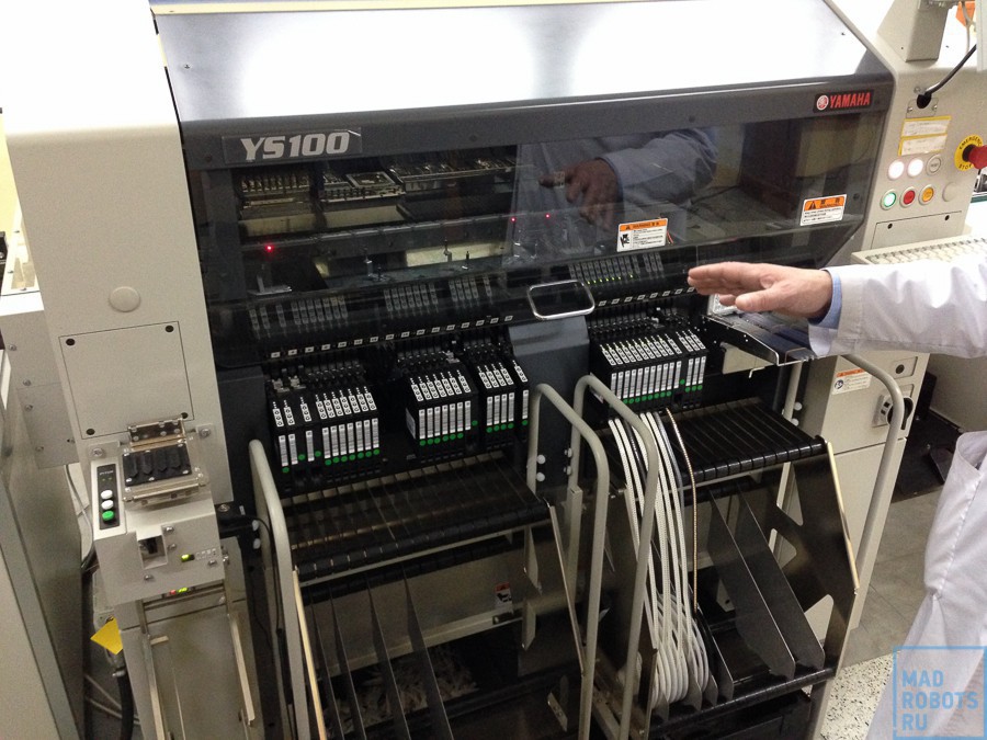
The template rises, and the solder paste is in the right places on the board. Cassettes with components are installed in the compartments:

Each component is inserted into its corresponding cassette: The

computer that controls the machine, says where what component is:
And he begins to arrange the components on the board.
It looks like this (video is not mine). You can watch forever:
The component installer is called the Yamaha YS100 and is capable of installing 25,000 components per hour (one spent 0.14 seconds).
Then the board goes through the hot and cold zones of the stove (cold - this means “only” 140 ° , as compared with 300 ° in the hot part). Having spent a strictly defined time in each zone with a strictly defined temperature, the solder paste melts, forming one whole with the legs of the elements and the printed circuit board: The
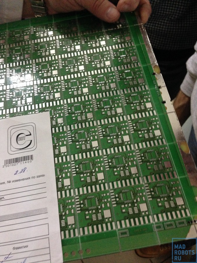
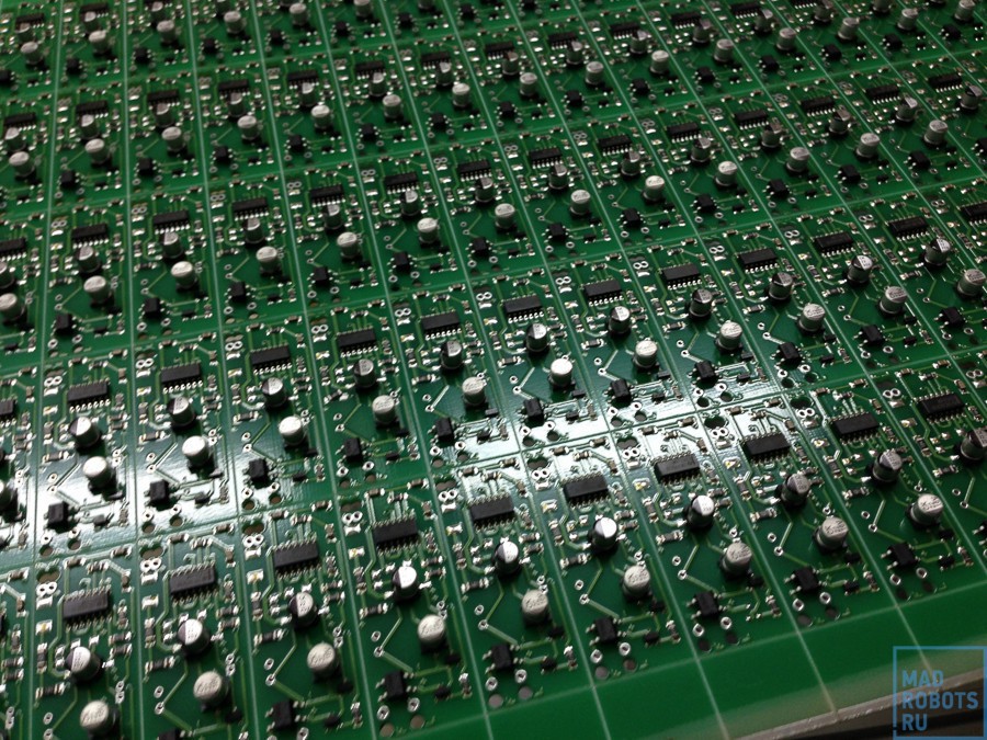
sealed sheet of boards looks like this:
Everything. The board is cut if necessary and packaged in order to soon leave for the customer:
Examples
Finally, examples of what tehnotech can do. For example, the design and manufacture of multi-layer circuit boards (up to 20 layers), including boards for BGA components and HDI boards:

the C with all the "license" military acceptance (yes, on each card manually put the number and date of production - this is required by the military):
Design, manufacturing and assembling boards of almost any complexity, from one’s own or from customer’s components:

And HF, UHF, boards with a metallized butt and a metal base (unfortunately, I didn’t take any photographs of this).
Of course, they are not a competitor to resonate in terms of fast prototype boards, but if you have from 5 pieces, I recommend asking them for the cost of manufacturing - they really want to work with civilian orders.
And yet, in Russia, production is still there. Whatever they say.
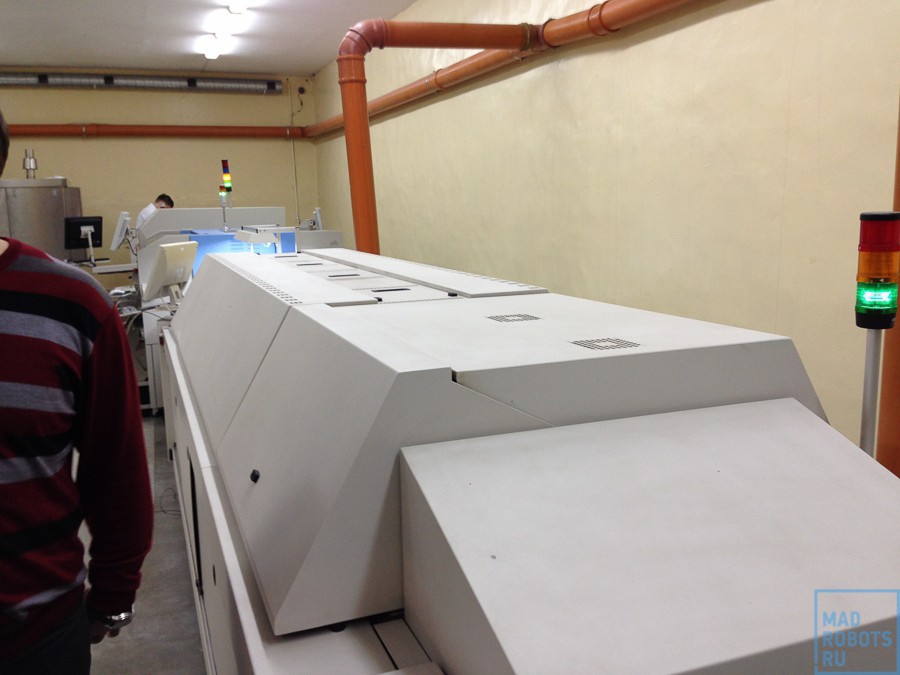
Finally, you can catch your breath, raise your eyes to the ceiling and try to understand the intricacies of the pipes:

What to read?
Subtractive combined positive method at home
DPP in pictures
Several different technologies for the manufacture of DPP and MPP
Production in photographs (but without a description)


So, how do we make circuit boards for our favorite gadgets?
The factory knows how to make boards from the beginning to the end - designing boards according to your TZ, making fiberglass, manufacturing single-sided and double-sided printed circuit boards, manufacturing multi-layer printed circuit boards, marking, checking, manual and automatic assembly and soldering of boards.
For starters, I'll show you how double-sided boards are made. Their technical process is no different from the production of single-sided printed circuit boards, except that in the manufacture of OPP do not perform operations on the second side.
About board making methods
In general, all methods for the manufacture of printed circuit boards can be divided into two broad categories: additive (from the Latin additio — addition) and subtractive (from the Latin subtratio — attention). An example of a subtractive technology is the well-known LUT (Laser-iron technology) and its variations. In the process of creating a printed circuit board using this technology, we protect future tracks on a sheet of fiberglass laminate with toner from a laser printer, and then bleed everything unnecessary in ferric chloride.In additive methods, conductive paths, on the contrary, are applied to the surface of the dielectric in one way or another.
Semiadditive methods (sometimes they are also called combined.) Are a cross between the classical additive and subtractive methods. In the process of producing PP according to this method, a part of the conductive coating can be etched (sometimes almost immediately after application), but as a rule it happens faster / easier / cheaper than in subtractive methods. In most cases, this is due to the fact that most of the thickness of the tracks is increased by electroplating or chemical methods, and the layer that is etched is thin, and serves only as a conductive coating for galvanic deposition.
I will show exactly the combined method.
')
Production of double-layer printed circuit boards using a combined positive method (semi-additive method)
Fiberglass fabrication
The process begins with the manufacture of foil fiberglass. Glass fiber is a material consisting of thin sheets of fiberglass (they look like a dense shiny fabric), impregnated with epoxy resin and pressed into a stack of sheets.Fiberglass cloths themselves are not too simple either - they are wicker (like ordinary fabric in your shirt) thin-thin strands of ordinary glass. They are so thin that they can easily bend in any direction. It looks like this:
You can see the orientation of the fibers on the long-suffering picture from Wikipedia:
In the center of the board, the light areas are fibers perpendicular to the shear, the areas are slightly darker - parallel.
Or, for example, on micrographs of tiberius , as I recall from this article:
So, let's begin.
Fiberglass cloth is supplied to production here in such reels:
It is already impregnated with partially cured epoxy resin - such a material is called a prepreg , from English pre- im preg nated - previously impregnated. Since the resin is already partially cured, it is no longer as sticky as it is in the liquid state - sheets can be picked up by hands, without being afraid to get dirty in the resin. The resin will become liquid only when the foil is heated, and then only for a few minutes before solidifying completely.
The required number of layers together with copper foil is collected on this machine:
But the foil roll itself.
Next, the canvas is cut into pieces and enters a press with a height of two human height:
On the photo is Vladimir Potapenko, production manager.
Interestingly, the heating technology was implemented during pressing: it was not the parts of the press that heated, but the foil itself. A current is supplied to both sides of the sheet, which, due to the resistance of the foil, heats the sheet of the future fiberglass. Pressing takes place under severely reduced pressure, to eliminate the appearance of air bubbles inside the PCB.
When pressing, due to heat and pressure, the resin softens, fills the voids and after polymerization a single sheet is obtained.
Here is this:
It is cut into blanks for boards with a special machine:
Technotech uses two types of blanks: 305x450 - a small group blank, 457x610 - a large blank
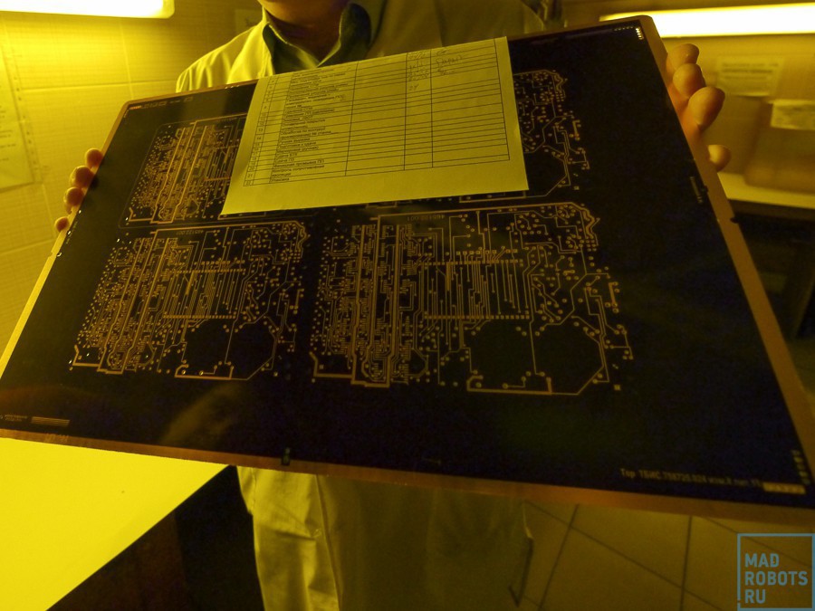
After that, for each set of blanks a route map is printed, and the journey begins ...
The route map is such a piece of paper with a list of operations, information about the board and a bar code. To control the execution of operations, 1C 8 is used, which contains all the information about orders, technical process, and so on. After the next production stage is completed, the barcode is scanned on the route list and entered into the database.
Drill blanks
The first stage of production of single-layer and two-layer printed circuit boards - drilling holes. With multilayer boards everything is more complicated, and I will tell about it later. Billets with route sheets arrive at the drill site:From blanks going package for drilling. It consists of a substrate (material such as plywood), from one to three identical pieces of printed circuit boards and aluminum foil. Foil is needed to determine if the drill touches the workpiece surface - this is how the machine determines the breakage of the drill. Even with each capture of the drill, he controls its length and sharpening with a laser.
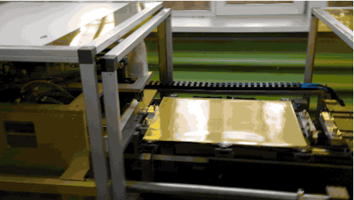
After the package is assembled, it is laid in this machine:
It is so long that I had to stitch this picture out of several frames. This is a Swiss machine company Posalux, the exact model, unfortunately I do not know. According to the characteristics it is close to this . He eats
The program is developed separately, and loaded over the network. All the operator needs to do is scan the barcode of the lot and lay a package of blanks inside. Capacity tool shop: 6000 drills or cutters.
Nearby there is a large cabinet with drills, but the operator does not need to monitor the sharpening of each drill and change it - the machine always knows the degree of wear of the drills - it records to itself how many holes were drilled by each drill. When the resource is exhausted, the drill itself changes to a new one; the old drill will be left unloaded from the container and sent for re-grinding.
Here is the interior of the machine:
After drilling in the route list and the base is a mark, and the fee is sent
Cleaning, activation of blanks and chemical copper plating.
Although the machine uses its “vacuum cleaner” during and after drilling, the surface of the board and the holes still need to be cleaned of dirt and prepared for the next process operation. For a start, the board is simply cleaned in the washing solution with mechanical abrasives.The inscriptions, from left to right, are: “Stripping chamber with brushes up / down”, “Washing chamber”, “Neutral zone”.
The fee becomes clean and shiny:
After this, the surface activation process is carried out in a similar installation.
After that, successively passing several baths in another similar installation, the billet acquires a thin (less than micron) layer of copper in the holes.
Further, this layer of electroplating increases to 3-5 microns - this improves the resistance of the layer to oxidation and damage.
Application and exposure of photoresist, removal of undelayed areas.
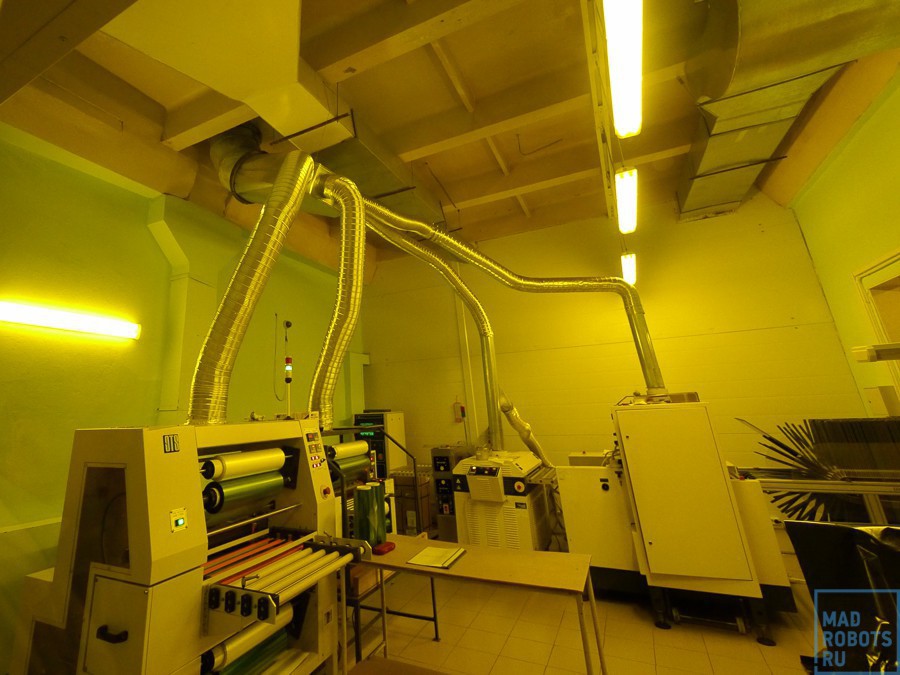
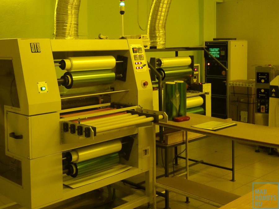
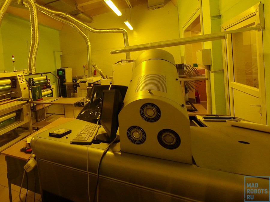
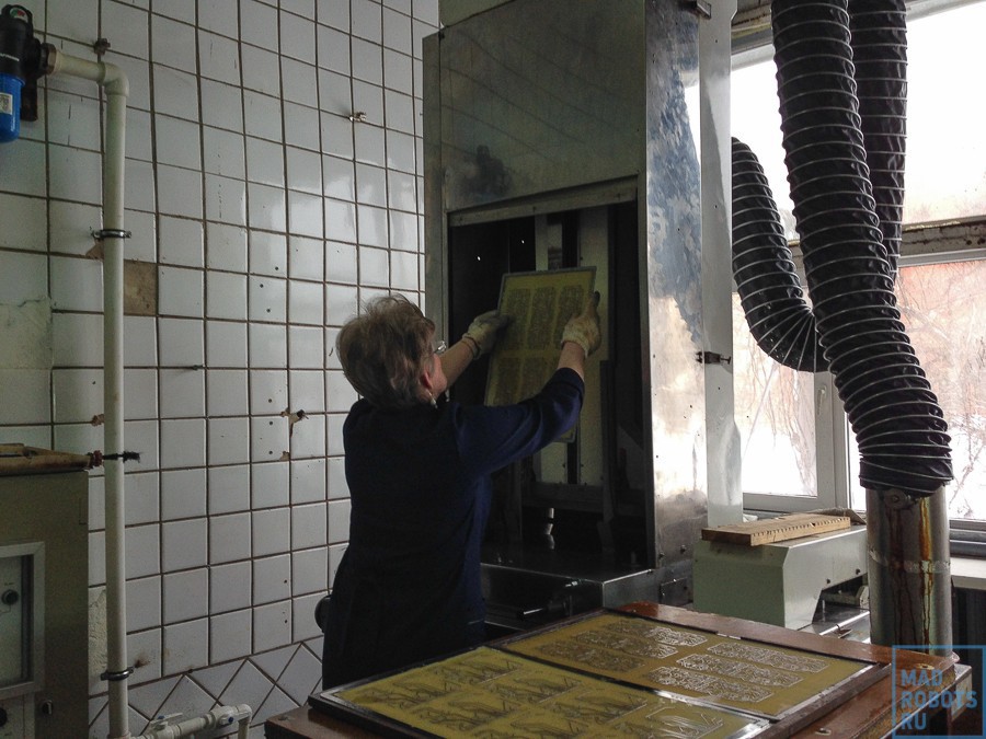
Then the board goes to the site of photoresist application. We were not allowed there, because it is closed, and in general, there is a clean room, so we confine ourselves to photographs through glass. I saw something similar in Half-Life (I’m talking about pipes coming down from the ceiling):Actually, here is the green film on the drum - this is the photoresist.
Further, from left to right (in the first photo): two settings for applying photoresist, then automatic and manual frames for illumination using previously prepared photomasks. In the automatic frame there is a control that takes into account the tolerance for alignment with reference points and holes. In the manual frame, the mask and the board are combined hands. Silkscreen and solder mask are displayed on the same frames. Next is the installation of developing and washing the boards, but since we did not get there, I don’t have photos of this part. But there is nothing interesting about the same conveyor as in the “activation”, where the workpiece passes successively several baths with different solutions.
And in the foreground is a huge printer that prints these same photo masks:
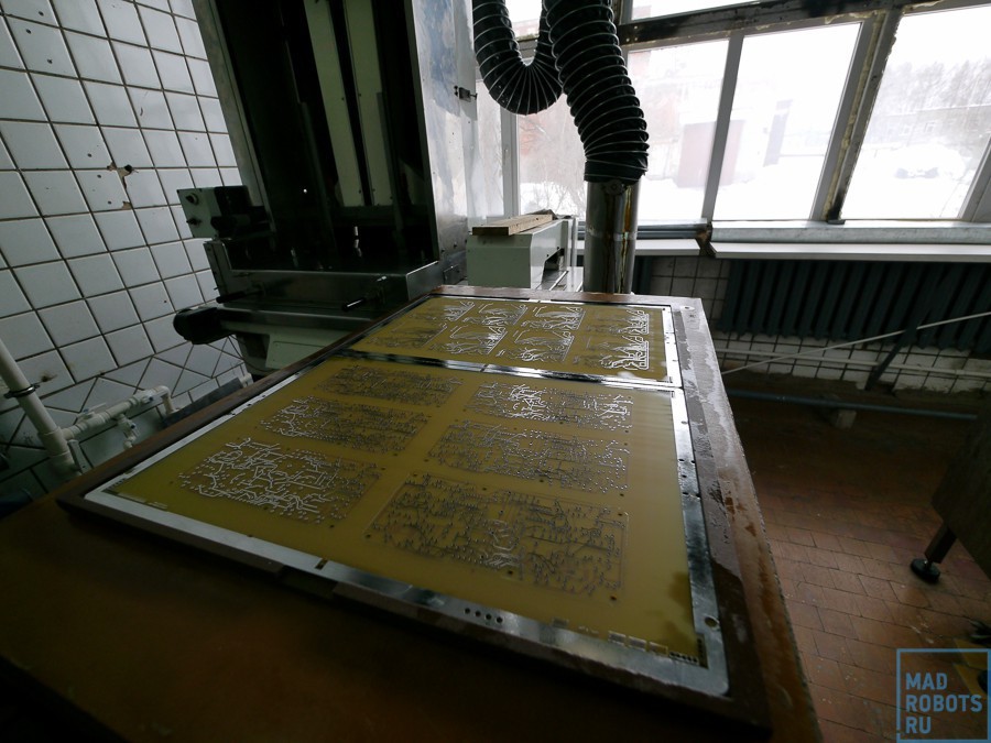
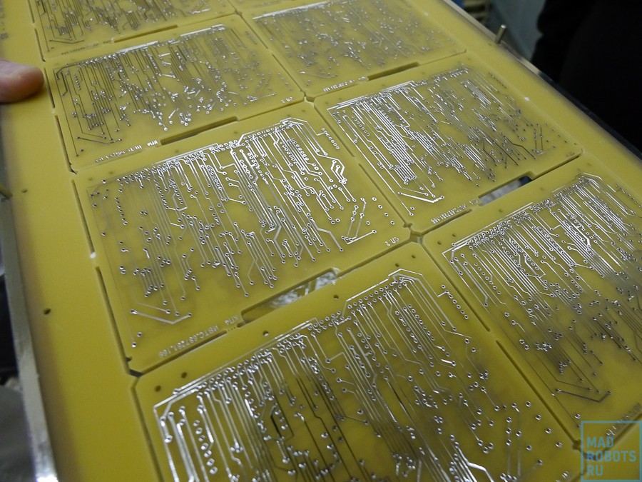
Here is a board with printed, exposed, and developed:
Please note that the photoresist is applied on the places where copper will not be in the future - the mask is negative and not positive, as in LUT or home photoresist. This is because in the future the build-up will take place at the locations of future tracks.
This is also a positive mask:
All these operations occur with nonactinic lighting, the spectrum of which is chosen in such a way as not to have an effect on the photoresist and to give maximum illumination for the work of a person in a given room.
I love ads, the meaning of which I do not understand:
Galvanic plating
Now came through her majesty - electroplating metallization. In fact, it was already carried out at the last stage, when a thin layer of chemical copper was growing. But now the layer will be increased even more - from 3 microns to 25. This is the layer that conducts the main current in the vias. This is done in such baths:In which complex electrolyte compositions circulate:
And a special robot, obeying a pledged program, drags boards from one bath to another:
One cycle of copper plating takes 1 hour and 40 minutes. 4 blanks can be processed in one pallet, but there can be several such pallet in the bath.
Deposition of metal resist
The next operation is another galvanic metallization, only now the deposited material is not copper, and the PIC is lead-tin solder. And the coating itself, by analogy with a photoresist, is called a metal resist. Boards are installed in the frame:This frame passes several electroplating baths already familiar to us:
And covered with a white layer of PIC. In the background you can see another board, not yet processed:
Removal of photoresist, etching of copper, removal of metalresist
Now the photoresist is washed off the boards, it has fulfilled its function. Now there are still metal-covered tracks on the still copper plate. At this installation etching occurs in a cunning solution, which etches copper, but does not touch the metal resist. As far as I remember, it consists of ammonium carbonate, ammonium chloride and ammonium hydroxide. After etching, the boards look like this:
The tracks on the board are a “sandwich” made from the bottom layer of copper and the top layer of the galvanic POS. Now, with another, even more tricky solution, another operation is carried out — the PIC layer is removed without affecting the copper layer.
However, sometimes the PIC is not removed, but melted in special furnaces. Or the board undergoes hot-dip (HASL-process) - when it sinks into a large solder bath. First, it is coated with rosin flux:
And here it is installed in this machine:
He lowers the board in a bath with solder and immediately pulls it back. Air flows blow off excess solder, leaving only a thin layer on the board. The fee is obtained like this:
But in fact, the method is a bit “barbaric” and does not really affect the boards, especially multi-layered ones — when immersed in the solder melt, the board suffers a temperature shock, which does not work very well on the internal elements of multi-layer boards and thin single- and double-layer tracks.
It is much better to cover with immersion gold or silver. Here is very good information about immersion coatings, if anyone is interested.
We did not visit the site of immersion coatings, for a banal reason - it was closed, and the key was too lazy. It's a pity.
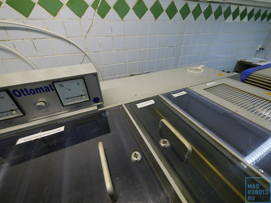
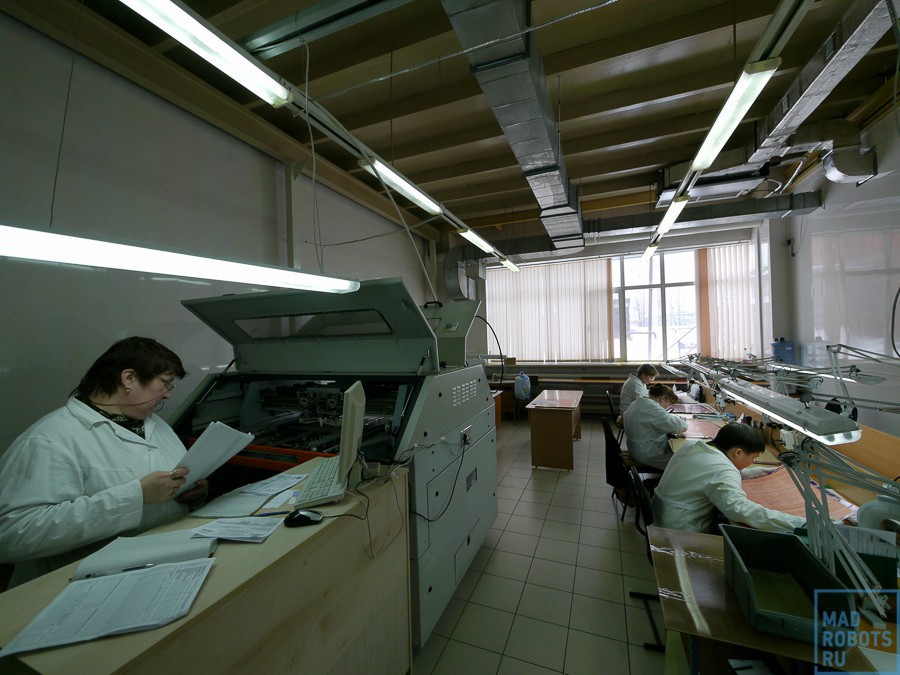
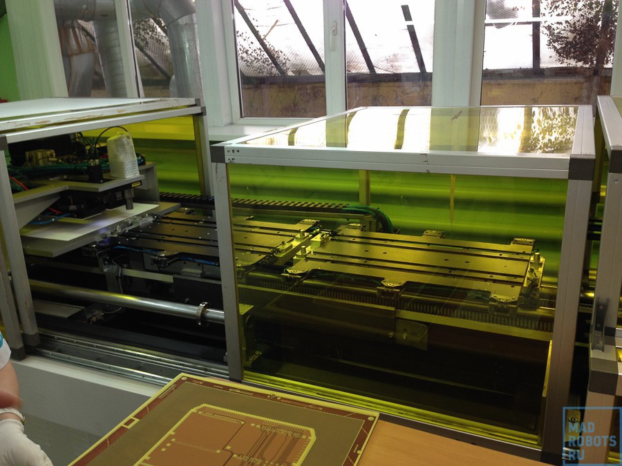
Electrotest
Then almost ready boards are sent for visual inspection and electrical test. Electric test is when the connections of all contact pads between themselves are checked, whether there are any breaks. It looks very funny - the machine holds the board and quickly pokes probes into it. You can watch the video of this process in my instagram (by the way, you can subscribe there). And in the form of a photo it looks like this:That big car on the left is an electric test. And here are the probes themselves closer:
In the video, however, there was another machine - with 4 probes, and here there are 16. They are said to be much faster than all three old machines with four probes combined.
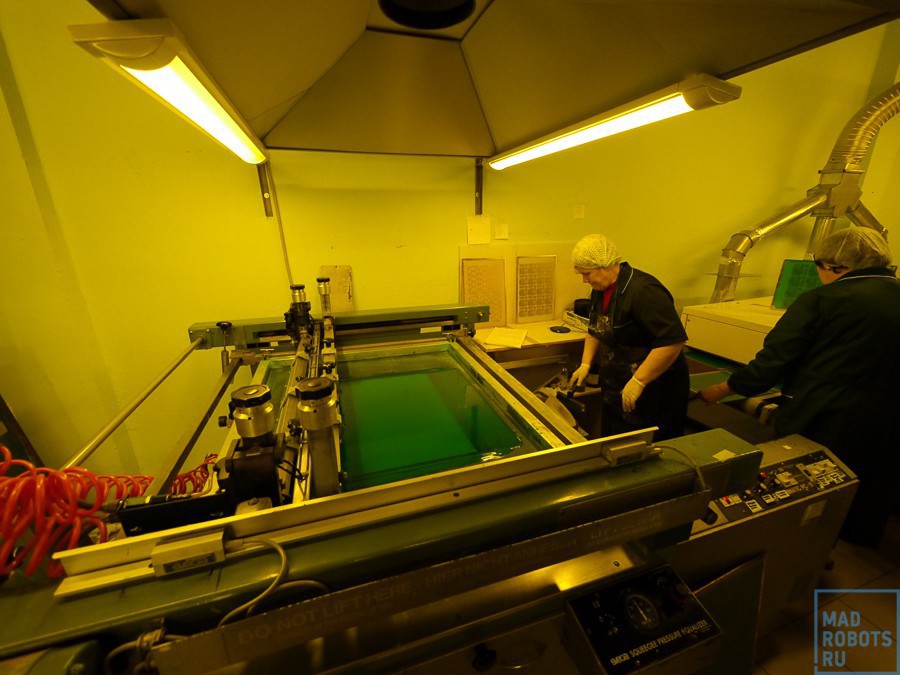
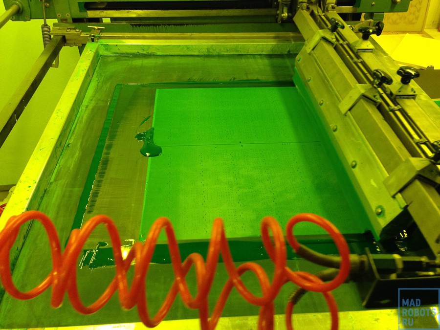
Application of solder mask and coating of contact pads
The next process is applying a solder mask. That is the greenest (well, most often greenish. In general, it comes in very different colors) the coating that we see on the surface of the boards. Prepared fees:Mounted here in this machine:
Which through a thin mesh spreads semi-fluid mask on the surface of the board:
Video drawing, by the way, can also be viewed in instagram (and subscribe too :)
After that, the boards dry until the mask stops sticking and are exhibited in the same yellow room that we saw above. After that, the unexposed mask is washed away, exposing the contact patches:
Then they are covered with a finishing coating - hot-dip or immersion coating:
And put the label - silk screen. These are white (most often) letters that show where a connector is and what element stands here.
It can be applied using two technologies. In the first case, everything is the same as with the solder mask, only the color of the composition is different. It covers the entire surface of the board, then it is exposed, and the areas uncured by ultraviolet light are washed away. In the second case, it is applied by a special printer printing with a cunning epoxy composition:
It is cheaper and much faster. The military, by the way, does not favor this printer, and constantly indicate in the requirements for their cards that the marking is applied only with a photopolymer, which is very distressing to the chief process engineer.
Production of multi-layer printed circuit boards by the method of metallization of through holes:
All that I have described above concerns only one-sided and double-sided printed circuit boards (at the factory, by the way, no one calls them that way, everyone says OPP and DPP). Multilayer boards (WFP) are made on the same equipment, but with a slightly different technology.Making cores
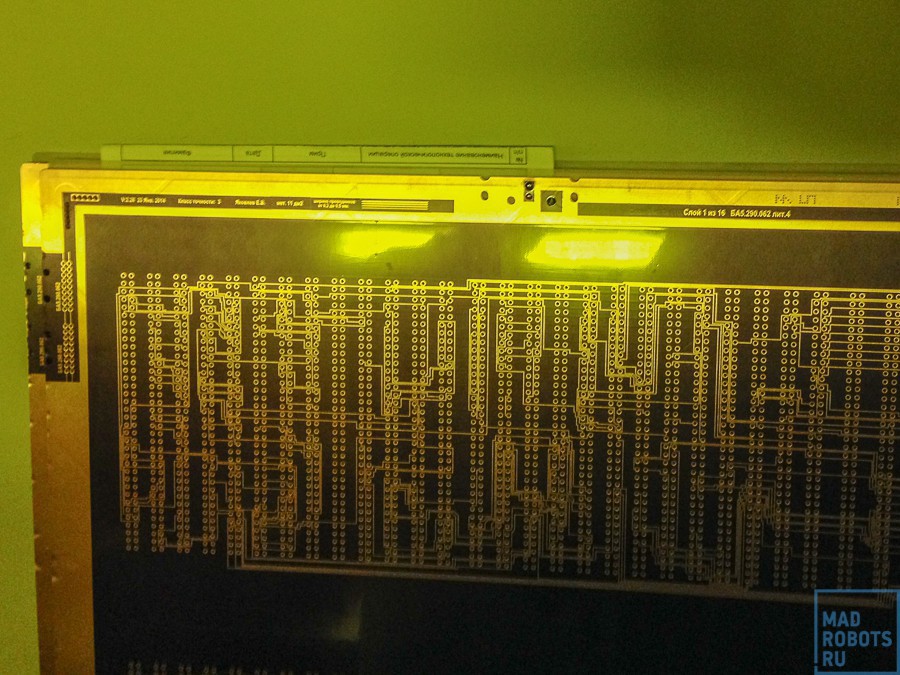
The core is the inner layer of a thin PCB with copper conductors on it. Such cores in the board can be from 1 (plus two sides - a three-layer board) to 20. One of the cores is called gold - this means that it is used as a reference layer - the layer along which all the others are exposed. The kernels look like this:They are made in the same way as conventional boards, only the thickness of the fiberglass laminate is very small - usually 0.5 mm. The sheet is so thin, it can be bent like thick paper. A copper foil is applied to its surface, and then all the usual stages occur - application, exposure of photoresist and etching. The result of this are the following sheets:
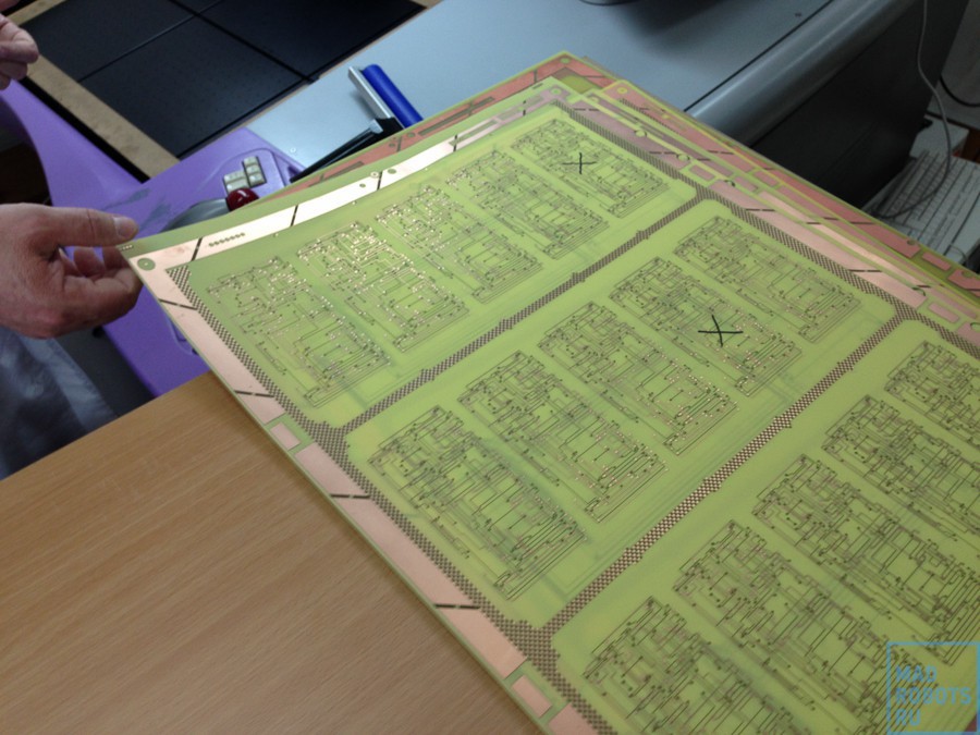
After manufacturing, the tracks are checked for integrity on the machine, which compares the board pattern to the clearance with the photo mask. In addition, there is also a visual control. And really visual - people are sitting and looking at the blanks:
Sometimes one of the control stages makes a verdict about the poor quality of one of the blanks (black crosses):
This sheet of boards, in which the defect occurred, will be made completely anyway, but after cutting the defective board will go to the garbage. After all the layers have been manufactured and tested, it is the turn of the next technological operation.
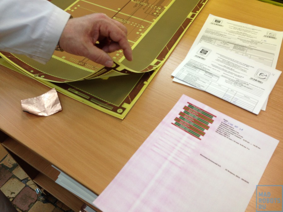
Assembly of the cores in the package and pressing
This takes place in the hall called “Plot pressing”:The cores for the board are laid out in this pile:
And next is a map of the location of the layers:
After that, the semi-automatic board pressing machine comes into play. Its semi-automaticity lies in the fact that the operator must, at her command, deliver the cores to it in a certain order.
Shifting them for insulation and bonding with prepreg sheets:
And then the magic begins. The machine captures and transfers sheets to the working field:
And then combines them along the reference holes relative to the gold layer.
Then the blank goes to a hot press, and after warming up and polymerization of the layers - to a cold one. After that we get the same sheet of fiberglass, which is no different from the blanks for double-layer printed circuit boards. But inside he has a
Drill blanks
When assembling an OPP and DPP package for drilling, it does not need to be centered, and it can be assembled with a certain tolerance - this is still the first technological operation, and everyone else will be guided by it. But when assembling a package of multilayer printed circuit boards, it is very important to bind to the inner layers - when drilling a hole must go through all the internal contacts of the cores, connecting them This is an X-ray drilling machine, which sees through the textolite the internal metallic reference marks and, by their location, drills the basic holes, into which the fasteners are inserted to install the package into the drilling machine.
Metallization
Then everything is simple - billets are drilled, cleaned, activated and metallized. The metallization of the hole interconnects all the copper heels inside the circuit board:Thus, completing the electronic circuit of the interior of the circuit board.
Check and grinding
Further a piece is cut from each board, which is polished and examined with a microscope in order to make sure that all the holes turned out to be normal.These pieces are called thin sections - transversely cut off parts of the printed circuit board, which allows you to evaluate the quality of the board as a whole and the thickness of the copper layer in the central layers and vias. In this case, under the thin section, they do not allow a separate payment, but the entire set of diameters of vias, specially made from the edge of the board, which are used in the order. The grout embedded in the transparent plastic looks like this:
Milling or scribing
Next, the boards that are on the group blank must be divided into several parts. This is done either on a milling machine:Which frezoy cuts the desired path.Another option is scribing, this is when the outline of the board is not cut, but is incised with a round knife. It is faster and cheaper, but allows you to make only rectangular boards, without complex contours and internal cuts. Here is a scribed board:
And here is a milled one:
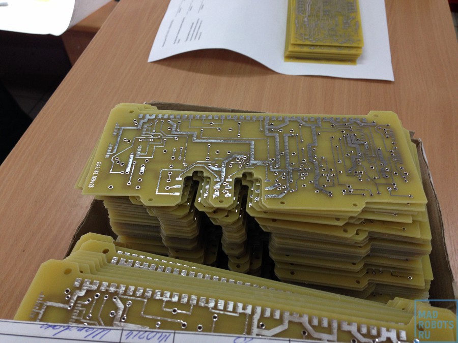
If only the production of boards was ordered, then this ends up - the boards are put in a pile: It turns
around with the same route list:
And it waits for sending.
And if assembly and sealing is needed, then there is still something interesting ahead.
Assembly
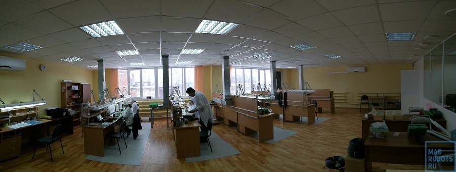
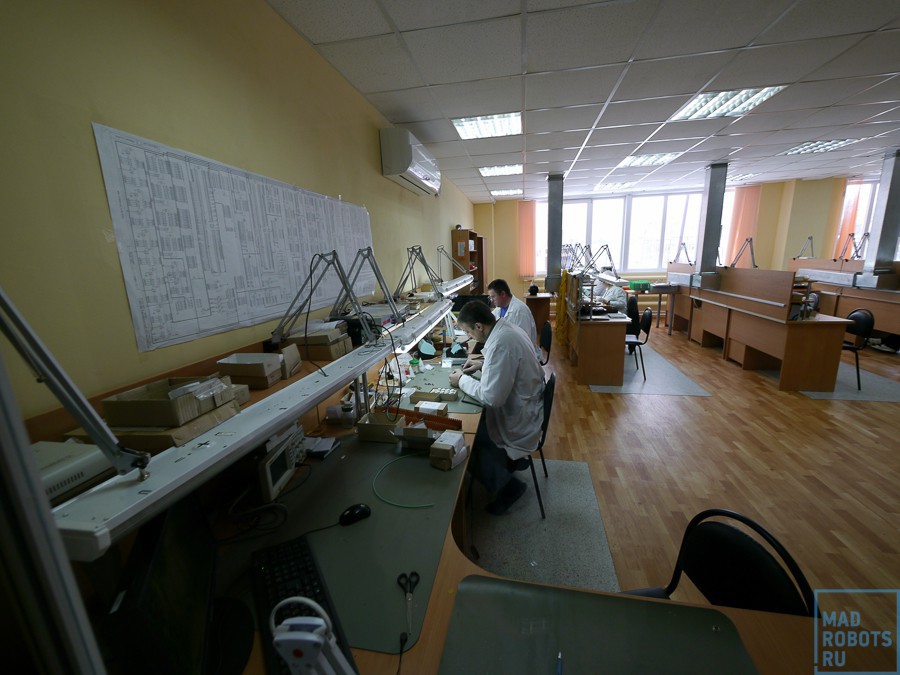
Then the board, if necessary, enters the assembly area, where the necessary components are soldered on it. If we are talking about manual assembly, then everything is clear, people are sitting (by the way, most of the women, when I went to them, my ears curled up from the tape song “God, what a man”):
And they collect, collect:
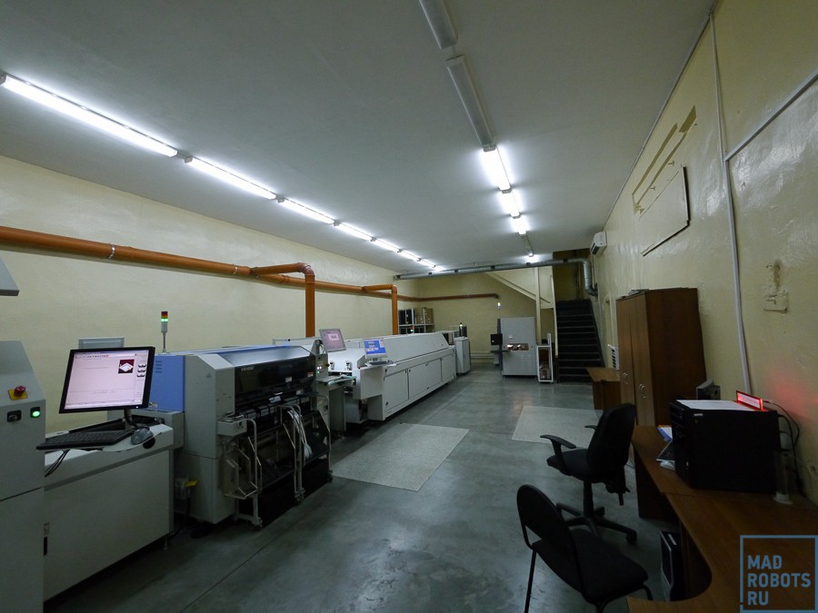
But if we talk about automatic assembly, then everything is much more interesting. It happens here on such a long 10-meter installation, which does everything - from applying solder paste to soldering on thermal profiles.
By the way, everything is serious. Even the mats are grounded there:
As I said, it all starts with the fact that the uncut sheet with printed circuit boards is installed with the metal template at the beginning of the machine. The solder paste is thickly smeared on the template, and the doctor blade passing from above leaves precisely measured quantities of paste in the cavities of the template.
The template rises, and the solder paste is in the right places on the board. Cassettes with components are installed in the compartments:
Each component is inserted into its corresponding cassette: The
computer that controls the machine, says where what component is:
And he begins to arrange the components on the board.
It looks like this (video is not mine). You can watch forever:
The component installer is called the Yamaha YS100 and is capable of installing 25,000 components per hour (one spent 0.14 seconds).
Then the board goes through the hot and cold zones of the stove (cold - this means “only” 140 ° , as compared with 300 ° in the hot part). Having spent a strictly defined time in each zone with a strictly defined temperature, the solder paste melts, forming one whole with the legs of the elements and the printed circuit board: The
sealed sheet of boards looks like this:
Everything. The board is cut if necessary and packaged in order to soon leave for the customer:
Examples
Finally, examples of what tehnotech can do. For example, the design and manufacture of multi-layer circuit boards (up to 20 layers), including boards for BGA components and HDI boards:the C with all the "license" military acceptance (yes, on each card manually put the number and date of production - this is required by the military):
Design, manufacturing and assembling boards of almost any complexity, from one’s own or from customer’s components:
And HF, UHF, boards with a metallized butt and a metal base (unfortunately, I didn’t take any photographs of this).
Of course, they are not a competitor to resonate in terms of fast prototype boards, but if you have from 5 pieces, I recommend asking them for the cost of manufacturing - they really want to work with civilian orders.
And yet, in Russia, production is still there. Whatever they say.
Finally, you can catch your breath, raise your eyes to the ceiling and try to understand the intricacies of the pipes:
What to read?
Subtractive combined positive method at homeDPP in pictures
Several different technologies for the manufacture of DPP and MPP
Production in photographs (but without a description)
Source: https://habr.com/ru/post/214153/
All Articles