Micron: A little more detailed about the production of 65nm microcircuits in Russia
 Yesterday, all domestic websites were flooded with the news that in Russia, Micron developed a technology for the production of microcircuits according to 65nm standards (or even “The first 65nm microchips were produced in Russia”). Previously, Micron had a 90nm technology licensed from STMicroelectronics. Let's try to sort out in more detail how things are going there.
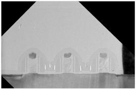
Micron this time surprisingly published a lot of information. The photographs show the layout of a single test transistor and photographs taken with an electron microscope. Under the cut, let's see how this could be done and compared with the Intel 65nm.
 |  |  |
Comparison of technical processes
Micron published a table with the parameters of their technical process. For comparison, I added Intel 65nm process technology:| Technology | Micron 65nm | Micron 90nm | Intel 65nm |
| Gate length | 45nm On the photo 54nm | 65nm | 35-38nm + Sige stress |
| Gate oxide thickness (electrical) | 2.2nm (n) / 2.2nm (p) | 2.2nm (n) / 2.2nm (p) | 1.2nm SiON |
| Interconnect | 9-Cu + 1-Al | 7-Cu + 1-Al | 8-Cu |
| Metal 1 pitch | 0.18µm | 0.24µm | 0.21µm |
| Inter-level dielectric | k = 2.9 | k = 2.9 | k = 2.9 |
The length of the gate and the thickness of the gate dielectric indicates that this LP process technology is of low consumption and slower operation. So, to make a processor similar to the first Core2Duo on Micron will not work out yet, but there are plenty of applications for LP technical processes.
')
The number of metals allows to implement processors of any complexity.
In pursuit of 65nm
As we remember , the resolution of optical photolithography is subject to Rayleigh criterion: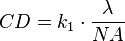
At the moment, the most advanced installation of photolithography on Micron (ASML PAS / 1150C scanner) has NA = 0.75 and operates at a wavelength of 193 nm. The parameter k is a multiplier of the “tricks” used to improve the resulting resolution. k for photolithography without tricks - 0.4. In the case of Mikronovskiy 90nm - k it was already 0.35. In order to get an honest 65nm with the same scanner, k would need to be somehow reduced to 0.25 (i.e., a lot of tricks should be added).
However, taking into account the words from the press release (“special algorithms for the introduction of optical correction of photolithography were developed”), the usual, classical topology of the test transistor (not using the “one-dimensional” structure) and the length of the gate in the photo (54nm) - at the moment looks just like the current equipment without additional tricks made the transistors with a smaller gate for the first tests (this dramatically increases the rejection rate, but for the test transistors is acceptable) + have worked out new technological steps of the process, about differing from 90nm.
They say that in March 2014 Micron is waiting for the arrival of a new scanner - and it will turn out 65nm without additional tricks, and with tricks - more subtle technical processes (45nm, lower?). Then, by the end of the year (or even in 2015), the first full-fledged microcircuits using 65nm technology will be released. The volume of production is expected to be about 500 200 mm plates per month - this almost guarantees that the production will be very expensive, and available only to the state.
Finally about possible tricks
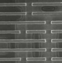 65nm can be obtained on the current equipment Micron. It is enough to recall how Intel in 2007 made the 45nm technical process on “dry” photolithography using a scanner with an aperture of 0.93 (I recall 0.75 from Micron): critical layers were exposed in 2 runs: on the first run they exposed a number of horizontal lines (using dipole illumination, polarization - so you can achieve a higher resolution, but only along one axis). Then the second exposure cut the lines into pieces of the desired shape. The result on the photo. Actually, in a similar way, the resolution is 32nm.
This approach allows us to obtain k = 0.21, and for the Mikronovsky scanner, this would allow to obtain a 55nm process technology. But certainly the amount of work would be very impressive.
Summary
- It’s still premature to talk about "65nm chips made in Russia" - these are single test transistors on existing equipment.
- LP technology (longer gate length, thicker gate dielectric) - with low consumption and slower speed, it is not worth expecting processors similar to Intel 65nm (first Core2Duo).
- With the new equipment (first of all, the scanner), which should be earned on Micron this year, 65nm technology and thinner ones will be possible.
- Due to the very small production volume (500 plates per month), the cost price of the plate promises to be quite high, and the market will not be able to fill up with a competitive civilian 65nm product. But this was not required.
Links
Press release MicronNews CNews with some additions
Intel 65nm Technology Overview
Comparative table of the whole heap of technologies
Source: https://habr.com/ru/post/213373/
All Articles