Radio-controlled switch do it yourself. Part 1 - Hardware
This post is the first part of a series of stories about how relatively easy it is to make a radio-controlled payload switch with your own hands.
The post is focused on beginners, for the rest, I think it will be a “repetition of the past”.
The approximate plan (we will look in the course of action) is expected the following:
At once I will make a reservation that the project is done for my specific needs, everyone can adapt it for themselves (all source codes will be presented in the course of the narration). In addition, I will describe these or other technological solutions and give their justifications.
Currently, the following inputs are available:
With the first point - everything is clear: normal desires must be satisfied.
')
The second point, in general, assumes that we need to make two different schemes (for a single and two-channel switch), but we act differently - we will make a “two-channel” module, but in the case when only one channel is really required, we will not unsolder part of the components on the board (we implement a similar approach in the code).
The third point - causes some flexibility in the choice of the switch form factor (the existing switch is actually removed, the installation box is dismantled, the finished device is mounted inside the wall, the installation box returns and the switch is mounted back).
The fourth point - greatly facilitates the search for a power source (220V is "at hand").
The inputs are clear, you can move on.
I want to make the switch multifunctional - i.e. the “tactile” component should remain (the switch should physically remain and its normal function of switching the load on / off should remain, but the possibility of controlling the load through the radio channel should appear.
To do this, the usual two-position (on / off) switches will be replaced by similar in design switches without latching (buttons):
These switches work primitively simple: when the key is pressed - a pair of contacts are closed, when the key is released - the contacts open. Obviously, this is the usual "clock button" (in fact, this is how we will process it).
Now it almost becomes clear how to implement it "in hardware":
The microcontroller will be used in the operating mode of the built-in oscillator - this will allow to abandon the external quartz resonator and a pair of capacitors (we will save a little and simplify the creation of the board and subsequent installation).
The radio channel will be organized using nRF24L01 +:
The module, as it is known, is tolerant to 5B signals at the inputs, but requires for power supply at 3.3V, respectively, in the circuit we will add a linear stabilizer L78L33 and a pair of capacitors to it.
Additionally, add blocking capacitors for power supply MK.
MK will be programmed via ISP - for this we will provide the corresponding connector on the module board.
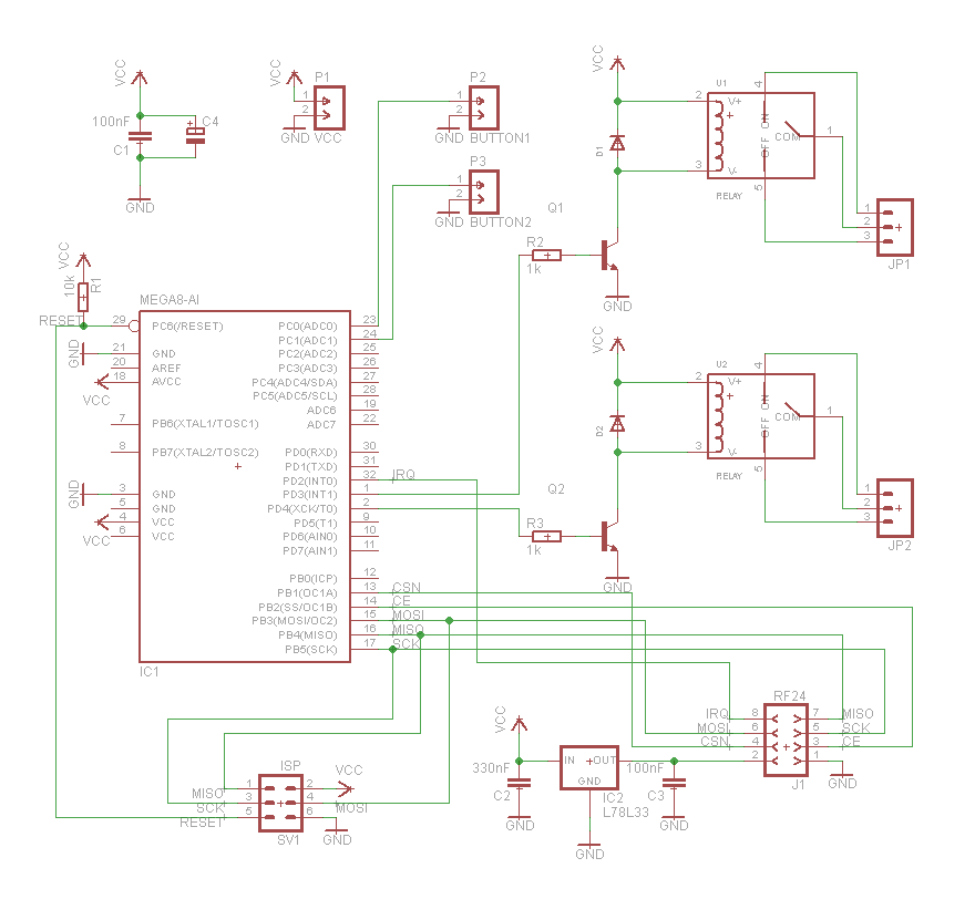
Actually, the whole scheme is described , it remains only to determine the conclusions of the MC, to which we will connect our "peripherals" (radio module, "buttons" and choose pins for controlling the relay).
Let's start with things that are actually defined:
It remains only to determine the pins for the buttons and transistors that control the relay. But let's not hurry - any MK pins (both digital and analog) will do for this. Select them at the board's trace stage (we’ll simply choose those pins that will be made as simple as possible to the corresponding “points”).
Now it is necessary to decide on what “corps” we will use. In this place my natural laziness begins to dictate the rules: I really do not like drilling printed circuit boards - so we will choose the maximum "surface mounting" (SMD). On the other hand, common sense suggests that using SMDs will greatly save PCB size.
Let's create a “shopping list” (BOM - bill of materials) for a “two-channel” module:
In addition to this, terminal blocks (for connecting the power load), a 2x4 block (for connecting a radio module), and a 2x3 connector (for ISP) are required.
Here I am a little tricky and peeping into my “vaults” (I just choose what is already there). You can choose components at your discretion (the choice of specific components is beyond the limits of this post).
Since the whole scheme is already practically “formed” (at least in the head), you can start designing our module.
For this we use the wonderful program - EAGLE .
In my opinion - very simple, but at the same time - a very convenient program for creating schematic diagrams and printed circuit boards for them. Additional "advantages" in the EAGLE piggy bank: multiplatform (I have to work on both Win- and MAC-computers) and the availability of a free version (with some limitations, which for the majority of home builders will seem completely insignificant).
Teaching you to use EAGLE in this topic is not included in my plans (at the end of the article there is a link to a great and very easy-to-learn tutorial on using EAGLE), I will only tell you some of my “tricks” when creating a board.
My algorithm for creating a circuit and a board was about the following (key sequence):
Scheme :
After these actions, we get a complete circuit, but so far the transistor switches and the “buttons” remain unconnected to the MC.
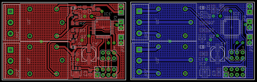
I proceed to the creation of the board (this time the thought went "from left to right"):
After the elements are placed in their places, I trace the conductors. “Land” (GND) - I’m not breeding (I will later make a range for this chain).
Now you can decide on the connection of keys and buttons (I see which pins are closer to the corresponding circuits and which will be easier to connect on the board), for this it is good to have the following picture before your eyes:
The location of the MK chip on the board is exactly the same as the picture above (it is only rotated 45 degrees clockwise), so my choice is as follows:
Actually, at this stage, the scheme takes the final form (we make the corresponding changes on the scheme - we “connect” the keys and buttons to the selected pins):
After that, I’m finishing the last connections in the PCB project, “throwing in” GND polygons (since the laser printer doesn’t print solid polygons badly, make it a “mesh”), add a couple of transitions (VIA) from one board layer to another and check that There is no chain left.
I got a scarf size 56h35mm.
Voila, you can begin to manufacture the PCB.
I make the pay using the LUT method (Laser-Iron Technology). At the end of the post there is a link to the materials that helped me a lot.
I will give for the order the main steps for making the board:
After it seems that all the paper has been removed, I wipe the board dry and under the light of a desk lamp I look for defects. Usually there are several places where pieces of glossy paper remain (look like whitish specks) - usually these residues are in the narrowest places between the conductors. I remove them with an ordinary sewing needle (a firm hand is important, especially in the manufacture of boards for "small" cases).
Further, the charge is persecuted in a solution of ferric chloride (avoiding under- and re-etching).
Toner wash off with acetone.

After that I do visual control (good lighting and a magnifier are required). If there are any suspicions that there is a “sticky” - control by the tester of “suspicious” places.
For complacency, the tester monitors all adjacent conductors (it is convenient to use the “dial” mode, when the tester gives an audible signal during “short circuit”).
If, after all, an unnecessary contact is found somewhere, I correct it with a sharp knife. Additionally, I draw attention to possible “microcracks” (for the time being I just fix them - I will correct it at the stage of board tinning).
I prefer to charge the board before drilling - so soft solder makes it a little easier to drill and the drill at the “exit” of the board less “tears” the copper conductors.
First, the printed circuit board must be degreased (acetone or alcohol), you can "walk" with an eraser to remove the oxides that have appeared. After that, I cover the board with regular glycerin and then already with a soldering iron (the temperature is somewhere around 300 degrees) with a small amount of solder “I drive” along the tracks - the solder lays down smoothly and beautifully (glitters). You need to tinker fast enough so that the tracks do not fall off.
When everything is ready, I launder the board with ordinary liquid soap.
After that, you can already drill a fee.
With holes with a diameter of more than 1mm, everything is quite simple (I just drill and that's all - you just have to try to keep the verticality, then the exit hole will fall into the place assigned to it).

But with vias (I make them with a 0.6mm drill) it is somewhat more difficult - the outlet, as a rule, turns out to be a bit “ragged” and this can lead to an undesirable rupture of the conductor.
Here you can advise to make each hole in two passes: drill first on one side (but so that the drill does not come out on the other side of the board), and then - similarly on the other side. With this approach, the "connection" of the holes will occur in the thickness of the board (and a small misalignment will not be a problem).
At first the interlayer jumpers are soldered.
Where it is just vias, I simply insert a piece of copper wire and seal it on both sides.
If the "transition" is carried out through one of the holes for the output elements (connectors, relays, etc.): I spread the stranded wire into thin strands and carefully solder pieces of this conductor from both sides in the holes where the transition is needed, while taking up minimal space inside the hole. This allows the transition to be realized and the holes remain sufficiently free so that the corresponding connectors normally fall into place and be unsoldered.
Here again, it is necessary to return to the “quality control” stage - I’m calling all previously suspicious and new places during tinning / drilling / creating transitions with a tester.
I check that the cracks found earlier are eliminated by solder (or by soldering a thin conductor over the cracks, if the crack remains after the tinning).
Eliminate all "zalipuhi", if such still appeared in the process of tinning. This is much easier to do now than debugging a fully assembled board.
Now you can proceed directly to the installation of elements.
My principle: “from the bottom up” (at first I unsolder the least high components, then those that are “higher” and those that are “high”). This approach allows placing all the elements on the board with less inconvenience.
Thus, SMD components are first decoupled (I start with those elements that have “more legs” - MK, transistors, diodes, resistors, capacitors), then it comes to output components - connectors, relays, etc.
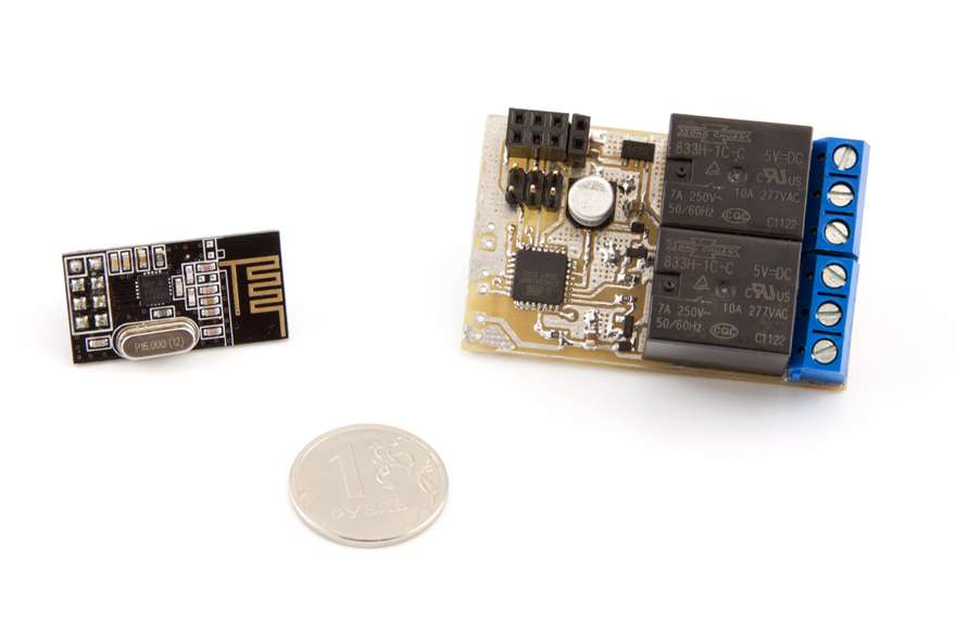
Thus, we get a ready-made fee.
To be continued ...
PS A “two-channel” module can be used to replace “walk-through” switches (usually placed at the beginning and end of a staircase between floors, etc.).
PPS If you use flatter pushbutton switches, then with a little refinement you can make boards that fit in existing installation boxes (that is, not only for placement in the niches of drywall walls).
PPPS Yes, this post is a development of the topic that I mentioned earlier .
Useful links :
The post is focused on beginners, for the rest, I think it will be a “repetition of the past”.
The approximate plan (we will look in the course of action) is expected the following:
- Switch hardware
- Testing and training
- Switch software
- "Control center"
At once I will make a reservation that the project is done for my specific needs, everyone can adapt it for themselves (all source codes will be presented in the course of the narration). In addition, I will describe these or other technological solutions and give their justifications.
Start
Currently, the following inputs are available:
- I want to implement remote control of light and exhaust.
- Switches have one- and two-section (light and light + hood).
- The switches are installed in a wall of plasterboard.
- All wiring is three-wire (there is a phase, zero, protective earth).
With the first point - everything is clear: normal desires must be satisfied.
')
The second point, in general, assumes that we need to make two different schemes (for a single and two-channel switch), but we act differently - we will make a “two-channel” module, but in the case when only one channel is really required, we will not unsolder part of the components on the board (we implement a similar approach in the code).
The third point - causes some flexibility in the choice of the switch form factor (the existing switch is actually removed, the installation box is dismantled, the finished device is mounted inside the wall, the installation box returns and the switch is mounted back).
The fourth point - greatly facilitates the search for a power source (220V is "at hand").
The inputs are clear, you can move on.
Principles and element base
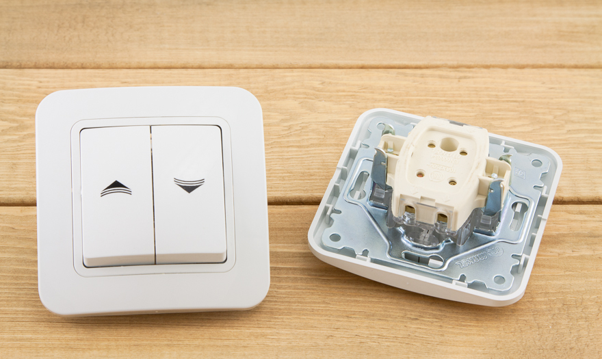
I want to make the switch multifunctional - i.e. the “tactile” component should remain (the switch should physically remain and its normal function of switching the load on / off should remain, but the possibility of controlling the load through the radio channel should appear.
To do this, the usual two-position (on / off) switches will be replaced by similar in design switches without latching (buttons):
These switches work primitively simple: when the key is pressed - a pair of contacts are closed, when the key is released - the contacts open. Obviously, this is the usual "clock button" (in fact, this is how we will process it).
Now it almost becomes clear how to implement it "in hardware":
- we take MK (atmega8, atmega168, atmega328 - I use what is "right now"), complete with MK we add a resistor for pulling RESET to VCC,
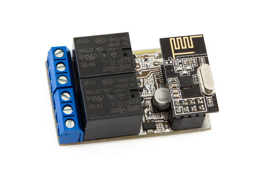
- We connect two “buttons” (to minimize the number of mounted elements, we will use pull-up resistors built into the MK), to switch the load, we will use the relay with the appropriate parameters (I just had 833H-1C-C relays with 5V control and enough switching power - 7A 250V ~),
- Naturally, it is impossible to directly connect the winding of the relay to the output of the MK (current is too high), therefore we will add the necessary “strapping” (resistor, transistor and diode).
The microcontroller will be used in the operating mode of the built-in oscillator - this will allow to abandon the external quartz resonator and a pair of capacitors (we will save a little and simplify the creation of the board and subsequent installation).
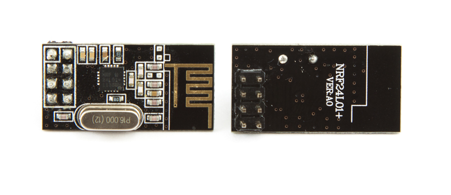
The radio channel will be organized using nRF24L01 +:
The module, as it is known, is tolerant to 5B signals at the inputs, but requires for power supply at 3.3V, respectively, in the circuit we will add a linear stabilizer L78L33 and a pair of capacitors to it.
Additionally, add blocking capacitors for power supply MK.
MK will be programmed via ISP - for this we will provide the corresponding connector on the module board.
Actually, the whole scheme is described , it remains only to determine the conclusions of the MC, to which we will connect our "peripherals" (radio module, "buttons" and choose pins for controlling the relay).
Let's start with things that are actually defined:
- The radio module is connected to the SPI bus (thus, we connect the pins of pads 1 to 8 on GND, 3V3, D10 (CE), D9 (CSN), D13 (SCK), D11 (MOSI), D12 (MISO), D2 (IRQ) - respectively).
- ISP is a standard thing and is connected as follows: we connect the connector pins 1 through 6 to D12 (MISO), VCC, D13 (SCK), D11 (MOSI), RESET, GND - respectively).
It remains only to determine the pins for the buttons and transistors that control the relay. But let's not hurry - any MK pins (both digital and analog) will do for this. Select them at the board's trace stage (we’ll simply choose those pins that will be made as simple as possible to the corresponding “points”).
Now it is necessary to decide on what “corps” we will use. In this place my natural laziness begins to dictate the rules: I really do not like drilling printed circuit boards - so we will choose the maximum "surface mounting" (SMD). On the other hand, common sense suggests that using SMDs will greatly save PCB size.
For beginners, surface mounting will seem like a rather complicated topic, but in reality it is not so scary (although with a more or less decent soldering station with a hairdryer). Youtube has a lot of video clips with lessons on SMD - I highly recommend reading it (I started using SMD myself a couple of months ago, I just learned from such materials).
Let's create a “shopping list” (BOM - bill of materials) for a “two-channel” module:
- microcontroller - atmega168 in a TQFP32 package - 1 pc.
- transistor - MMBT2222ALT1 in the SOT23 package - 2 pcs.
- diode - 1N4148WS in a SOD323 package - 2 pcs.
- stabilizer - L78L33 in SOT89 package - 1 pc.
- Relay - 833H-1C-C - 2 pcs.
- 10kΩ resistor, size 0805 - 1 pc. (RESET lift to VCC)
- 1kOhm resistor, size 0805 - 1 pc. (in the base circuit of the transistor)
- capacitor - 0.1µF, size 0805 - 2 pcs. (on nutrition)
- capacitor - 0.33µF, size 0805 - 1 pc. (on nutrition)
- electrolytic capacitor - 47 microfarads, size 0605 - 1 pc. (on nutrition)
In addition to this, terminal blocks (for connecting the power load), a 2x4 block (for connecting a radio module), and a 2x3 connector (for ISP) are required.
Here I am a little tricky and peeping into my “vaults” (I just choose what is already there). You can choose components at your discretion (the choice of specific components is beyond the limits of this post).
Since the whole scheme is already practically “formed” (at least in the head), you can start designing our module.
In general, it would be nice to first assemble everything on a breadboard (using cases with lead elements), but since I have all the above described “nodes” already repeatedly tested and implemented in other projects, let me skip the design stage.
Design
For this we use the wonderful program - EAGLE .
In my opinion - very simple, but at the same time - a very convenient program for creating schematic diagrams and printed circuit boards for them. Additional "advantages" in the EAGLE piggy bank: multiplatform (I have to work on both Win- and MAC-computers) and the availability of a free version (with some limitations, which for the majority of home builders will seem completely insignificant).
Teaching you to use EAGLE in this topic is not included in my plans (at the end of the article there is a link to a great and very easy-to-learn tutorial on using EAGLE), I will only tell you some of my “tricks” when creating a board.
My algorithm for creating a circuit and a board was about the following (key sequence):
Scheme :
- We create a new project, inside which we add a “scheme” (empty file).
- Add MK and the necessary "weight" (pull-up resistor on the RESET, blocking capacitor for power, etc.). Pay attention to the hull (Package) when selecting items from the library.
- "Picture" the key on the transistor that controls the relay. We copy this piece of the scheme (for the organization of the "second channel"). The entrances of the keys - while leaving the "hang in the air."
- Add an ISP connector and a block to connect the radio module to the circuit (we make the corresponding connections in the circuit).
- To power the radio module, add a stabilizer to the circuit (with appropriate capacitors).
- We add “connectors” for connecting “buttons” (one pin of the connector is immediately “grounded”, the second one is “dangling in the air”).
After these actions, we get a complete circuit, but so far the transistor switches and the “buttons” remain unconnected to the MC.
I proceed to the creation of the board (this time the thought went "from left to right"):
- Placing the terminal blocks to connect the power load.
- To the right of the terminal blocks - relay.
- More to the right - elements of transistor switches.
- The power supply stabilizer for the radio module (with the corresponding capacitors) is placed next to the transistor switches (at the bottom of the board).
- I place the block for connecting the radio module to the bottom right (we pay attention to what position the radio module itself will have when connected correctly to this block - according to my idea it should not protrude beyond the limits of the main board).
- The ISP connector is placed next to the radio module connector (since the same “pins” of the MK are used - to make it easier to part the board).
- In the remaining space I have the MK (the body must be “twisted” in order to determine its most optimal position in order to ensure the minimum length of the tracks).
- The blocking capacitors are placed as close as possible to the corresponding terminals (MC and radio module).
After the elements are placed in their places, I trace the conductors. “Land” (GND) - I’m not breeding (I will later make a range for this chain).
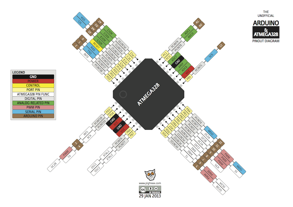
Now you can decide on the connection of keys and buttons (I see which pins are closer to the corresponding circuits and which will be easier to connect on the board), for this it is good to have the following picture before your eyes:
The location of the MK chip on the board is exactly the same as the picture above (it is only rotated 45 degrees clockwise), so my choice is as follows:
- We connect transistor switches to pins D3, D4.
- Buttons - on A1, A0.
The attentive reader will see that atmega8 appears on the diagram below, atmega168 is mentioned in the description, and amega328 is shown in the picture with the chip. Let it not confuse you - the chips have the same pinout and (specifically for this project) are interchangeable and differ only in the amount of memory “on board”. Choose what you like / is there (I later soldered 168 “pebbles” into the board: more memory than amega8 - it will be possible to implement more logic, but this is in the second part).
Actually, at this stage, the scheme takes the final form (we make the corresponding changes on the scheme - we “connect” the keys and buttons to the selected pins):
After that, I’m finishing the last connections in the PCB project, “throwing in” GND polygons (since the laser printer doesn’t print solid polygons badly, make it a “mesh”), add a couple of transitions (VIA) from one board layer to another and check that There is no chain left.
I got a scarf size 56h35mm.
The archive with the scheme and the board for Eagle version 6.1.0 (and higher) is located here .
Voila, you can begin to manufacture the PCB.
PCB manufacturing
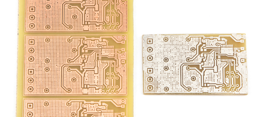
I make the pay using the LUT method (Laser-Iron Technology). At the end of the post there is a link to the materials that helped me a lot.
I will give for the order the main steps for making the board:
- I print on Lomond 130 paper (glossy) the underside of the board.
- I print on the same paper the upper side of the board (mirror!).
- I fold the resulting printouts with the images inside and on the lumen I combine (it is very important to get maximum accuracy).
- After that, using a stapler, fasten sheets of paper (constantly checking that the combination is not broken) from three sides - it turns out to be an “envelope”.
- I cut a suitable size piece of double-sided fiberglass (with metal or scissors scissors).
- Steklotekstolit needs to be treated with very fine sandpaper (we remove oxides) and degrease (I make it with acetone).
- The resulting blank (neatly, by the edges, without touching the cleaned surfaces) is placed in the resulting “envelope”.
- I warm up the iron "to the fullest" and carefully iron the workpiece from two sides.
- I leave the board to cool (5 minutes), then you can soak the paper under a stream of water and remove it.
After it seems that all the paper has been removed, I wipe the board dry and under the light of a desk lamp I look for defects. Usually there are several places where pieces of glossy paper remain (look like whitish specks) - usually these residues are in the narrowest places between the conductors. I remove them with an ordinary sewing needle (a firm hand is important, especially in the manufacture of boards for "small" cases).
Further, the charge is persecuted in a solution of ferric chloride (avoiding under- and re-etching).
Toner wash off with acetone.
Tip : when you make small boards, make a blank for the required number of boards, simply by placing the images of the top and bottom of the board in several copies - and already this “combined” image “roll” onto the fiberglass laminate. After etching, it will be sufficient to cut the blank into separate boards.
Just be sure to check the dimensions of the boards when entering on paper: some programs like to “zoom in” slightly when outputting, and this is unacceptable.
Quality control
After that I do visual control (good lighting and a magnifier are required). If there are any suspicions that there is a “sticky” - control by the tester of “suspicious” places.
For complacency, the tester monitors all adjacent conductors (it is convenient to use the “dial” mode, when the tester gives an audible signal during “short circuit”).
If, after all, an unnecessary contact is found somewhere, I correct it with a sharp knife. Additionally, I draw attention to possible “microcracks” (for the time being I just fix them - I will correct it at the stage of board tinning).
Tinning drilling
I prefer to charge the board before drilling - so soft solder makes it a little easier to drill and the drill at the “exit” of the board less “tears” the copper conductors.
First, the printed circuit board must be degreased (acetone or alcohol), you can "walk" with an eraser to remove the oxides that have appeared. After that, I cover the board with regular glycerin and then already with a soldering iron (the temperature is somewhere around 300 degrees) with a small amount of solder “I drive” along the tracks - the solder lays down smoothly and beautifully (glitters). You need to tinker fast enough so that the tracks do not fall off.
When everything is ready, I launder the board with ordinary liquid soap.
After that, you can already drill a fee.
With holes with a diameter of more than 1mm, everything is quite simple (I just drill and that's all - you just have to try to keep the verticality, then the exit hole will fall into the place assigned to it).
But with vias (I make them with a 0.6mm drill) it is somewhat more difficult - the outlet, as a rule, turns out to be a bit “ragged” and this can lead to an undesirable rupture of the conductor.
Here you can advise to make each hole in two passes: drill first on one side (but so that the drill does not come out on the other side of the board), and then - similarly on the other side. With this approach, the "connection" of the holes will occur in the thickness of the board (and a small misalignment will not be a problem).
Mounting elements
At first the interlayer jumpers are soldered.
Where it is just vias, I simply insert a piece of copper wire and seal it on both sides.
If the "transition" is carried out through one of the holes for the output elements (connectors, relays, etc.): I spread the stranded wire into thin strands and carefully solder pieces of this conductor from both sides in the holes where the transition is needed, while taking up minimal space inside the hole. This allows the transition to be realized and the holes remain sufficiently free so that the corresponding connectors normally fall into place and be unsoldered.
Here again, it is necessary to return to the “quality control” stage - I’m calling all previously suspicious and new places during tinning / drilling / creating transitions with a tester.
I check that the cracks found earlier are eliminated by solder (or by soldering a thin conductor over the cracks, if the crack remains after the tinning).
Eliminate all "zalipuhi", if such still appeared in the process of tinning. This is much easier to do now than debugging a fully assembled board.
Now you can proceed directly to the installation of elements.
My principle: “from the bottom up” (at first I unsolder the least high components, then those that are “higher” and those that are “high”). This approach allows placing all the elements on the board with less inconvenience.
Thus, SMD components are first decoupled (I start with those elements that have “more legs” - MK, transistors, diodes, resistors, capacitors), then it comes to output components - connectors, relays, etc.
Thus, we get a ready-made fee.
To be continued ...
PS A “two-channel” module can be used to replace “walk-through” switches (usually placed at the beginning and end of a staircase between floors, etc.).
PPS If you use flatter pushbutton switches, then with a little refinement you can make boards that fit in existing installation boxes (that is, not only for placement in the niches of drywall walls).
PPPS Yes, this post is a development of the topic that I mentioned earlier .
Useful links :
Source: https://habr.com/ru/post/211126/
All Articles