IBM will use DNA to self-assemble future chips
IBM employees have developed a fundamentally new concept for assembling future generations of chips. Instead of traditional photolithography, it is planned to assemble chip structures based on informational DNA-carrying molecules. Theoretically, this approach will allow using synthesis to greatly increase the performance of the microcircuits. IBM experts are planning to complete the technology rollout in 10-20 years.

Article translation
')
While other manufacturers in search of ways to reduce the size of computer chips equip them with an increasing number of transistors, IBM specialists are engaged in a comprehensive solution to the problem - the creation of processors that use DNA (digital network architecture).
For the past year and a half, IBM has been working on designing a new platform for the location of transistors and connections inside the processor.
Today, semiconductor manufacturers use optical lithography (optical lithography), which uses light to transmit the form. The problem, according to Joe Gordon, chief specialist of materials for advanced technologies, is that it is very difficult to shrink the platform using existing technologies.
And since, as Gordon said, a 50% improvement in processor performance comes at the expense of “shrinking”, shrinking the platform, scientists need to invent a new way to create a platform.
The role and importance of DNA
“At this stage, the development of the industry will allow us to work in a processor with elements of 22 nano-meters in size,” says Gordon. - Now we are looking for opportunities to go even further. It is clear that it will not be easy to create something even smaller in size using optical lithography, as we know it. And DNA will help us do that. ”
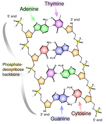
IBM staffer Greg Wallof (Greg Wallraff) explained that researchers have single DNA molecules on the surface of the chip and use them as a template for assembling electronic components such as nano-lamps and nano-wires. By the way, DNA used by engineers came from viruses, Greg Wollorff added.
Greg Wollorff noted that the IBM research team is collaborating with Paul Rothemund of the California Institute of Technology, who once developed a method for assembling DNA molecules into a complex structure. Based on this research, IBM scientists are trying to turn DNA into suitable platforms.
“People call DNA a project for life,” Vorof continues. - Specific DNA structures have unique properties. DNA is programmable in principle. You can design DNA into unique forms with its own specific junction points. Then, we pour this DNA form into a silicone substrate, and the DNA is built exactly according to our desire, and finally, we assemble the remaining components of the system. ”
The junction points on the DNA, which are located at the points where the nano-wires and the transistors were supposed to join the platform, can be located much closer to each other than in the traditional processor fabrication scheme. With DNA, the joints lag behind each other by a distance of 4-6 nano-meters. Traditionally, this value is about 45 nano-meters.
“Imagine the process of covering tiling. And the DNA particles are exactly this tile, ”explains Gordon. - Each tile has a specific set of electronic components. These tiles are located on the chip more freely, so that their number reaches thousands and millions. The second step, which we still do not know how to do, is to connect them together. We have already taken up dimensions that are much more impressive than in the framework of traditional lithography. ”
After the nano-lamps and nano-wires are laid on the platform, the DNA should be extracted.
Wolrof believes that a single chip will require millions of DNA platforms.
Gordon notes that the team of researchers is far from being able to comprehend and calculate to the end the whole process of introducing the DNA model into action. "We still do not exactly imagine how all this will work," said the researcher. - How do we make the "tiles" connect and attach in the right places? Can we use nano-wires to attach them to the "tiles" at the required points? Can we tie them? ”
Wolrof said that the next step would be to connect all the “tiles” together and identify weak points in their connection.
Indeed, using this technique, we will probably move forward 10 or 20 years ahead ...
Article translation
')
While other manufacturers in search of ways to reduce the size of computer chips equip them with an increasing number of transistors, IBM specialists are engaged in a comprehensive solution to the problem - the creation of processors that use DNA (digital network architecture).
For the past year and a half, IBM has been working on designing a new platform for the location of transistors and connections inside the processor.
Today, semiconductor manufacturers use optical lithography (optical lithography), which uses light to transmit the form. The problem, according to Joe Gordon, chief specialist of materials for advanced technologies, is that it is very difficult to shrink the platform using existing technologies.
And since, as Gordon said, a 50% improvement in processor performance comes at the expense of “shrinking”, shrinking the platform, scientists need to invent a new way to create a platform.
The role and importance of DNA
“At this stage, the development of the industry will allow us to work in a processor with elements of 22 nano-meters in size,” says Gordon. - Now we are looking for opportunities to go even further. It is clear that it will not be easy to create something even smaller in size using optical lithography, as we know it. And DNA will help us do that. ”
IBM staffer Greg Wallof (Greg Wallraff) explained that researchers have single DNA molecules on the surface of the chip and use them as a template for assembling electronic components such as nano-lamps and nano-wires. By the way, DNA used by engineers came from viruses, Greg Wollorff added.
Greg Wollorff noted that the IBM research team is collaborating with Paul Rothemund of the California Institute of Technology, who once developed a method for assembling DNA molecules into a complex structure. Based on this research, IBM scientists are trying to turn DNA into suitable platforms.
“People call DNA a project for life,” Vorof continues. - Specific DNA structures have unique properties. DNA is programmable in principle. You can design DNA into unique forms with its own specific junction points. Then, we pour this DNA form into a silicone substrate, and the DNA is built exactly according to our desire, and finally, we assemble the remaining components of the system. ”
The junction points on the DNA, which are located at the points where the nano-wires and the transistors were supposed to join the platform, can be located much closer to each other than in the traditional processor fabrication scheme. With DNA, the joints lag behind each other by a distance of 4-6 nano-meters. Traditionally, this value is about 45 nano-meters.
“Imagine the process of covering tiling. And the DNA particles are exactly this tile, ”explains Gordon. - Each tile has a specific set of electronic components. These tiles are located on the chip more freely, so that their number reaches thousands and millions. The second step, which we still do not know how to do, is to connect them together. We have already taken up dimensions that are much more impressive than in the framework of traditional lithography. ”
After the nano-lamps and nano-wires are laid on the platform, the DNA should be extracted.
Wolrof believes that a single chip will require millions of DNA platforms.
Gordon notes that the team of researchers is far from being able to comprehend and calculate to the end the whole process of introducing the DNA model into action. "We still do not exactly imagine how all this will work," said the researcher. - How do we make the "tiles" connect and attach in the right places? Can we use nano-wires to attach them to the "tiles" at the required points? Can we tie them? ”
Wolrof said that the next step would be to connect all the “tiles” together and identify weak points in their connection.
Indeed, using this technique, we will probably move forward 10 or 20 years ahead ...
Source: https://habr.com/ru/post/21105/
All Articles