IBM plans to move to a new type of integrated circuit

Jon Casey, IBM Semiconductor Research and Development Center
The other day, John Casey, an employee of IBM's Center for Semiconductor Research and Development, gave a very interesting interview. In it, Casey announced that IBM is looking for worthy alternatives to CMOS technology and von Neumann architecture, since Moore’s law is slowing down and something qualitatively new is needed.
John Casey himself is not a person from the outside, he has a very high qualification in the field of technologies for creating integrated circuits. Casey took part in some very interesting projects, including one of the latest projects: the study of the possibility of technology leaving the limits of Moore's law. It was this topic that became the keynote speaker at the symposium of John Casey, which was devoted to the industry strategy of the International Association of Semiconductor Equipment and Materials SEMI in California (USA).
')
Before the performance, the author gave an interview to the EE Times, presenting the main theses of his report. Casey expressed support for the views of Bernie Meyerson, who also gave an interview to the EE Times , just recently. “A lot of articles are being written about the imminent death of Moore’s law, and even specific dates are called. That is why there is a shift towards new types of architecture, which can be called information-centric, since the data sets in such systems are simply huge, ”says Casey.
Among other things, now there is a change in approaches to the production of chips and devices.
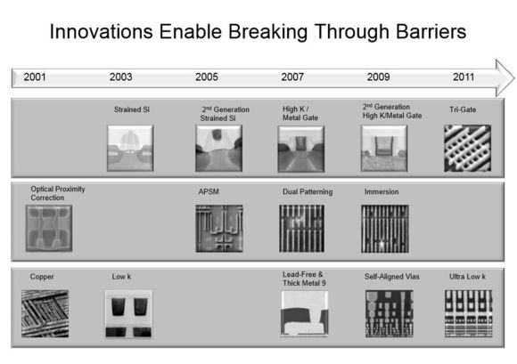
However, the transition to 450-mm silicon wafers and hard ultraviolet lithography (EUV) will not happen very soon, because there is an important role to play another factor - economic feasibility. Initially, a transition will be made to the bulk or the so-called heterogeneous miniaturization, at the level of the integrated circuit, in order to achieve higher performance, as well as economic efficiency from further miniaturization.
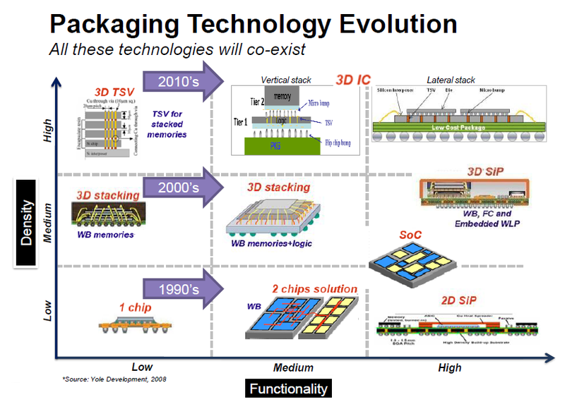
John Casey believes that one of the best solutions in this case is 3D integration, which provides very high values of I / O speed. So, according to Casey, you should use the now traditional 3D stack of two active chips. The first advantage of implementing such a solution is greater density. The second advantage is an increase in access speed and the ability to optimize I / O speed.
These parameters, in turn, can be improved by improving the materials themselves, their layout and order of joints (in order to reduce the length of the joints). And 3D is a great opportunity for this.
There is also another option - this is 2.5D integration, this option is now being considered and discussed by the company's specialists. 2.5D integration can be realized on the basis of silicon, organic compound or glass. And now all of these opportunities are being actively checked, tested under heavy loads and large amounts of data.
The advantage of a 2.5D solution can be that this method allows combining chips with various manufacturing techniques to produce a module with high performance and not a very high final price. The use of three chips in the complex is mentioned, with the first 45-nm control chip of a silicon-on-insulator with a CMOS processor chip and two 130-nm SiGe transistor transceivers mounted on a substrate on a silicon interposer.
As a result, a productive and functional transceiver of mixed signals is obtained, where the data transfer rate between the chips is 2 Tbit / s. And this is a very significant achievement, which may be the answer to the question “How to ensure speed in the conditions of slowing down Moore's law”.
Source: https://habr.com/ru/post/210774/
All Articles