Nanotechnology for everyone. Part 1: How and what to measure the nanoscale? Scanning tunneling microscopy
Greetings to you, glorious inhabitants of Habrogorod!
The pluses in the comments in the IBM post and the answers to my question in the Toasterand also the karma that grew 3 times during the night indicated Habr's bright desire to read popular science articles: deep enough, but written in human language and with transparent analogies. Define in advance how and what we will write.
In the posts will not:
The publications will be:
There is a lot of material and to enhance learning it’s better to start with an engineering article. So, how to understand what technology is in front of us, nano or not? Let's measure it.
First of all, we note that I think rather a technologist and experimenter, therefore, with great disapproval, I treat people who use the mathematical apparatus, not understanding the essence of the process and the nature of the physics of the phenomena studied.
Let's forget about the fashion brand "nanotechnology" and high-pair definitions. Nano is one of the prefixes of scale. No different from micro or mega. Thus, it is logical to assume that if we can operate in technologies with objects of a size comparable to a millimeter (for example, turning parts on a lathe), then this is millitechnology.
')
Let's try to present the nanoscale and one billionth of a meter. The thickness of a human hair (by the way, depends on its color) is tens of micrometers. The nanoscale begins if we reduce this thickness by 10,000 (!) Times. Take a hair in your hands and evaluate its width by eye. I suggest you reduce it mentally. Hard to imagine? And I did not say that it is just (frankly, impossible at all).
It turns out to be easier to measure than imagined. Physics is generally surprising in that it’s constantly explaining impossible analogies to explain things that cannot be imagined to explain nature.
To measure the room footage is better to use a tape measure. Ipad'a width is more convenient to measure using a ruler. The thickness of the factory parts perfectly measured with a caliper. And the thickness of the hair can be seen on an optical (school) microscope.
But how to measure a nano object?
Any measurement is based on the concept of comparison with the standard. How does this happen?
There are no other methods for direct measurement of length (or I cannot remember). It is important to understand that direct measurements are actions when the result is the directly sought value. Of course, I can measure the thickness of the glass, focusing on the change in the intensity of the light passing through it (the thicker the glass - the less light). I measure the intensity of light, and then I indirectly calculate the thickness for some dependencies. As you might guess, these are indirect measurements.
Can we impose a reference nano object on another? Of course not. Can we visually compare? We can, but it is very difficult (due to the nature of the light. The explanation and methods for circumventing the natural limitations will be in the following article).
If we can't imagine and see, then let's ... feel !
In 1981, a scanning tunneling microscope or STM was invented. The idea is as follows: we take a gramophone with a thin conducting needle and place the probe above the sample (there is no touch).
Photograph of scanning probe microscopy
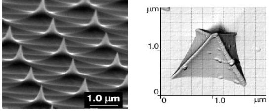
On the device we detect the current, since the electric circuit is closed (electrons jump from the surface to the needle, the so-called tunnel effect). If the probe passes over the pit - see the weakening of the current. If under the probe slide - gain. This is due to changes in the distance between the needle and the sample. Based on the data, we build pictures (the contrast depends on the amount of current at a particular point. The lighter - the higher the values, since the probe was closer to the surface).
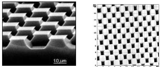
On the left, we observe a photograph taken with the help of optical methods (scale of 10 micrometers), on the right there is an image obtained using STM. Funny, but there is no color and can not be. All pictures from the microworld are painted by hand for pop clarity. On a nanoscale, the concept of color simply disappears.
Simple and beautiful, isn't it? Let's do it at home. We extract all the necessary tools, sharpen the needle.
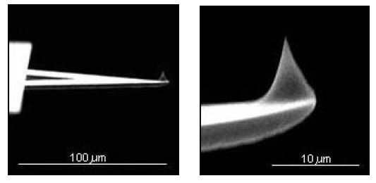
Scientifically, not a needle, but a cantilever. By the way, its thickness at the end can reach 10 nm. How to do this? Question on a separate article. In the meantime, let's say Santa Claus gave you;)
The question arises how to bring the needle close enough to the surface (about 0.1 - 1 nanometers) and not accidentally touch the sample?

To measure the nanoscale you first need to learn how to move objects with nanofiber. In modern probe microscopes, the accuracy of the probe retention is 0.001 nanometers! If an industrial robot had a similar displacement accuracy with dimensions of about one meter, then with a needle clamped in the manipulators, he could draw a circle with a diameter of several nanometers. Fantastic, in short.
Fortunately, there is a way out - piezoelectric elements. Depending on the current flowing through itself, the size of such elements varies in “nanos”. A quick and direct analogy is temperature expansion. If we heat the metal - it changes its size, imperceptibly to the eye, but noticeable for engineering structures. The "piezo" the same property, but with an electric current.
It turns out, if we attach a probe to such an element, let us down with a microscope at a distance of 1 μm, then let the current through the “piezo” - we will overcome another 0.99 μm and be close to the surface, as required! Problem solved. We can start measurements.
There are several measurement modes in probe microscopy:
When the cantilever is scanning the surface, we can raise the probe while increasing the current (to reduce the tunnel effect) or lower it to strengthen it. Thus, we strive for DC mode depending on the height. The needle always has one level of approach to the surface, that is, we carefully “feel” the sample.
And we can fix the height of the needle and move it only in horizontal directions, focusing on the change in current. This is a constant height mode. This is convenient if the sample is fairly uniform in height — we can quickly “run” parallel to the surface and remove current data.
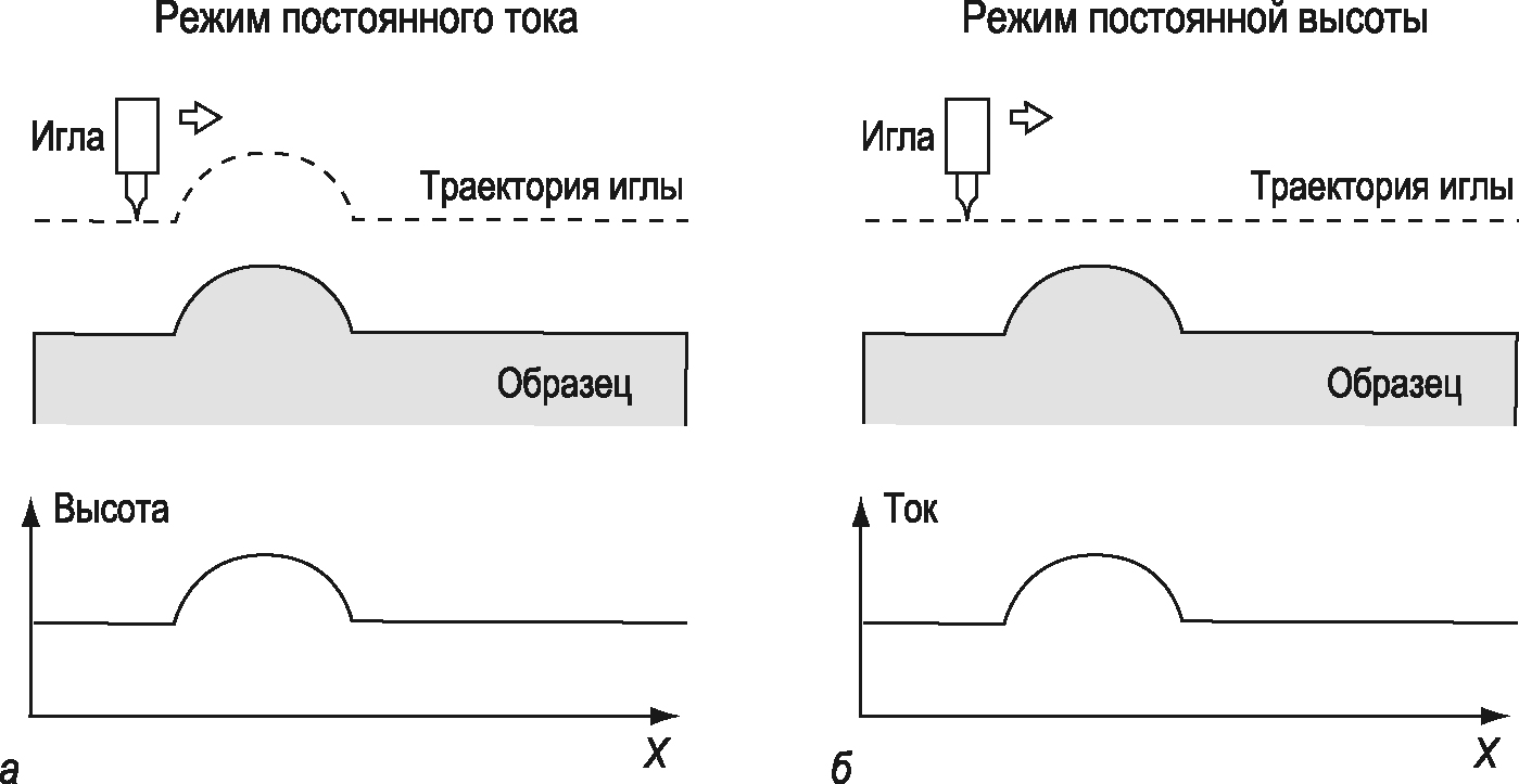
The scheme of work with the surface in different modes.
Anyway, we can always unambiguously determine the height of the object.
But how to measure its width, or scientific language, lateral size? As you understand, this is not about huge hills like in the previous picture, but about objects the size of several nanometers.

Here is our nanoobject on the table.

And here is the same object next to the tip of the cantilever.
It is reasonable that when the probe moves to the left, the ball will begin to touch the probe from the side , and not from below. A smooth ascent, an exit to a maximum (when the ball is exactly under the tip of the probe), then a smooth descent begins. Is it obvious that we will get a smooth curve hill (the dependence of the height of the probe raising on the coordinate), in which the height is clearly visible, and the width is smeared regardless of the shape and thickness of the nanoobject?
Thus, we can only estimate the lateral size, but the accuracy of the determination is much lower than the height measurements.
Of course, there are still many subtleties and nuances that have no special value for non-specialists. Let's take stock.
Advantages of STM:
Disadvantages of STM:
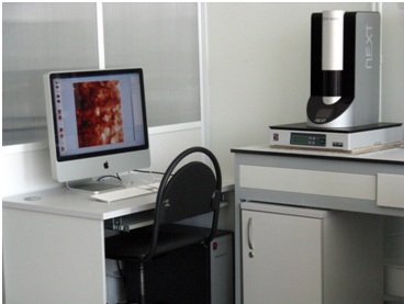
Photo installation STM. The price on the Internet is not so easy to find, but be guided by 6 zeros in ruble equivalent, depending on the configuration.
All scanning probe microscopes (SPM) at the core of the method use the types of exposure of the probe to the surface.
In the next article I will talk about the natural evolution of the STM and how to benefit from the gravitational forces, why the probe oscillates and what is the difficulty in measuring tiny angles.
Catch a beautiful picture at last:
The pluses in the comments in the IBM post and the answers to my question in the Toaster
In the posts will not:
- repetitions of knowledge from Wikipedia and popular science cranberries with statements "taken from the ceiling";
- mathematics and formulas. At all;
- educational program about the school course of physics.yes it is not difficult for me, but then the article will grow to the size of a female whale; D. We are all adults and if we don’t understand the basics, we’ll look for the answer ourselves or ask in the comments.
The publications will be:
- emphasis on technical and engineering part;
- many questions. I wanted the reader to turn on his brain and try to think like a researcher;
- A large number of visual pictures.
There is a lot of material and to enhance learning it’s better to start with an engineering article. So, how to understand what technology is in front of us, nano or not? Let's measure it.
Magic ruler
First of all, we note that I think rather a technologist and experimenter, therefore, with great disapproval, I treat people who use the mathematical apparatus, not understanding the essence of the process and the nature of the physics of the phenomena studied.
My teachers
Unfortunately, education in our country works according to the principle: MUCH a lot of mathematics and the lack of visual comparisons. With this paragraph, I want to express my recognition and gratitude to my teachers, who (amazingly!) Did not stuff with the formulas in the last courses of the institute, but explained the essence of physics on their fingers. Their names: I.S. Vasilyevsky, V.A. Kulbachinsky and legendary V.P. Gladkov, who taught us to think after several years of cerebral impotence.
Let's forget about the fashion brand "nanotechnology" and high-pair definitions. Nano is one of the prefixes of scale. No different from micro or mega. Thus, it is logical to assume that if we can operate in technologies with objects of a size comparable to a millimeter (for example, turning parts on a lathe), then this is millitechnology.
')
Let's try to present the nanoscale and one billionth of a meter. The thickness of a human hair (by the way, depends on its color) is tens of micrometers. The nanoscale begins if we reduce this thickness by 10,000 (!) Times. Take a hair in your hands and evaluate its width by eye. I suggest you reduce it mentally. Hard to imagine? And I did not say that it is just (frankly, impossible at all).
It turns out to be easier to measure than imagined. Physics is generally surprising in that it’s constantly explaining impossible analogies to explain things that cannot be imagined to explain nature.
To measure the room footage is better to use a tape measure. Ipad'a width is more convenient to measure using a ruler. The thickness of the factory parts perfectly measured with a caliper. And the thickness of the hair can be seen on an optical (school) microscope.
But how to measure a nano object?
Any measurement is based on the concept of comparison with the standard. How does this happen?
- Visual comparison: We can find a pebble the size of a micrometer, put it on the table of a microscope, look, draw a scale of measurements on the lens and look at it for further research.
- Overlay: Take a ruler or roulette, we know its exact size. We attach it to the sample, look how many times the object fits on the ruler, we calculate the desired length.
There are no other methods for direct measurement of length (or I cannot remember). It is important to understand that direct measurements are actions when the result is the directly sought value. Of course, I can measure the thickness of the glass, focusing on the change in the intensity of the light passing through it (the thicker the glass - the less light). I measure the intensity of light, and then I indirectly calculate the thickness for some dependencies. As you might guess, these are indirect measurements.
Can we impose a reference nano object on another? Of course not. Can we visually compare? We can, but it is very difficult (due to the nature of the light. The explanation and methods for circumventing the natural limitations will be in the following article).
If we can't imagine and see, then let's ... feel !
Probe microsocopy. STM principles
In 1981, a scanning tunneling microscope or STM was invented. The idea is as follows: we take a gramophone with a thin conducting needle and place the probe above the sample (there is no touch).
Photograph of scanning probe microscopy
On the device we detect the current, since the electric circuit is closed (electrons jump from the surface to the needle, the so-called tunnel effect). If the probe passes over the pit - see the weakening of the current. If under the probe slide - gain. This is due to changes in the distance between the needle and the sample. Based on the data, we build pictures (the contrast depends on the amount of current at a particular point. The lighter - the higher the values, since the probe was closer to the surface).
On the left, we observe a photograph taken with the help of optical methods (scale of 10 micrometers), on the right there is an image obtained using STM. Funny, but there is no color and can not be. All pictures from the microworld are painted by hand for pop clarity. On a nanoscale, the concept of color simply disappears.
Simple and beautiful, isn't it? Let's do it at home. We extract all the necessary tools, sharpen the needle.
Scientifically, not a needle, but a cantilever. By the way, its thickness at the end can reach 10 nm. How to do this? Question on a separate article. In the meantime, let's say Santa Claus gave you;)
The question arises how to bring the needle close enough to the surface (about 0.1 - 1 nanometers) and not accidentally touch the sample?
To measure the nanoscale you first need to learn how to move objects with nanofiber. In modern probe microscopes, the accuracy of the probe retention is 0.001 nanometers! If an industrial robot had a similar displacement accuracy with dimensions of about one meter, then with a needle clamped in the manipulators, he could draw a circle with a diameter of several nanometers. Fantastic, in short.
Fortunately, there is a way out - piezoelectric elements. Depending on the current flowing through itself, the size of such elements varies in “nanos”. A quick and direct analogy is temperature expansion. If we heat the metal - it changes its size, imperceptibly to the eye, but noticeable for engineering structures. The "piezo" the same property, but with an electric current.
It turns out, if we attach a probe to such an element, let us down with a microscope at a distance of 1 μm, then let the current through the “piezo” - we will overcome another 0.99 μm and be close to the surface, as required! Problem solved. We can start measurements.
Measurements and New Problems
There are several measurement modes in probe microscopy:
When the cantilever is scanning the surface, we can raise the probe while increasing the current (to reduce the tunnel effect) or lower it to strengthen it. Thus, we strive for DC mode depending on the height. The needle always has one level of approach to the surface, that is, we carefully “feel” the sample.
And we can fix the height of the needle and move it only in horizontal directions, focusing on the change in current. This is a constant height mode. This is convenient if the sample is fairly uniform in height — we can quickly “run” parallel to the surface and remove current data.
The scheme of work with the surface in different modes.
Anyway, we can always unambiguously determine the height of the object.
But how to measure its width, or scientific language, lateral size? As you understand, this is not about huge hills like in the previous picture, but about objects the size of several nanometers.
Here is our nanoobject on the table.
And here is the same object next to the tip of the cantilever.
It is reasonable that when the probe moves to the left, the ball will begin to touch the probe from the side , and not from below. A smooth ascent, an exit to a maximum (when the ball is exactly under the tip of the probe), then a smooth descent begins. Is it obvious that we will get a smooth curve hill (the dependence of the height of the probe raising on the coordinate), in which the height is clearly visible, and the width is smeared regardless of the shape and thickness of the nanoobject?
Thus, we can only estimate the lateral size, but the accuracy of the determination is much lower than the height measurements.
Conclusion
Of course, there are still many subtleties and nuances that have no special value for non-specialists. Let's take stock.
Advantages of STM:
- measurement accuracy is 0.1 - 10 nm (I could not find the data on the Internet, and notebooks are far away. I can be a little mistaken, pointing out from memory).
- no direct effects on the sample (do not damage the surface, other methods are not so loyal).
Disadvantages of STM:
- measures only conductive samples (therefore, often organic matter is sprayed with gold in order to “see”).
- for a very long time (I remember sitting in the laboratory for 40 minutes while scanning a small area measuring several tens of micrometers. The longer the measurement, the more accurate and better the picture).
- weak definition of lateral sizes.
Photo installation STM. The price on the Internet is not so easy to find, but be guided by 6 zeros in ruble equivalent, depending on the configuration.
All scanning probe microscopes (SPM) at the core of the method use the types of exposure of the probe to the surface.
In the next article I will talk about the natural evolution of the STM and how to benefit from the gravitational forces, why the probe oscillates and what is the difficulty in measuring tiny angles.
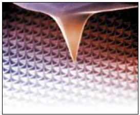
Catch a beautiful picture at last:
Source: https://habr.com/ru/post/205956/
All Articles