Bitcoin: development history, ASIC
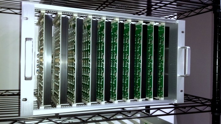
Bitcoin-miner from ASICMINER, performance ~ 2TH / s (source)
The previous part.
This time we will consider the final part of the history of the development of computing systems intended for bitcoin mining, namely the ASIC era, which put an end to GPU and FPGA miners.
Butterfly Labs (BFL)
BFL was the first company to announce its miner based on ASIC. Confidence in success was largely based on the previous achievements of this company in the field of FPGA-miners.
In June 2012, BFL began to accept pre-orders for three types of miners: $ 149 for Jalapenos, with a capacity of 4.5 GH / s; $ 1299 for SC Singles at 60GH / s; and for $ 30K it was possible to pre-order the MiniRigs monster SC with a performance of 1500GH / s.
At this price, these miners could extract 20-50 times more bitcoins per dollar investment than GPU or FPGA miners. The amount of pre-orders only for the first day increased $ 250K and the activity of customers remained high for a long time. This turned out to be more than enough to cover the substantial costs of chip design and manufacture of lithographic masks for the 65nm process technology, which are estimated at $ 500K.
Each BFL chip contains 16 fully deployed pipelines for computing the SHA256, which is equivalent in performance to 16 mid-hi-end FPGAs fit in 1 ASIC. At the same time, the chip size was only 10x10mm in the BGA package.
')
But then SUDDENLY! ... Initially, the BFL planned to begin deliveries of miners in early November. However, the deadlines were shifted many times due to delays associated with production at the factory, assembly and problems of the BFL itself. Also, the power consumption at the level of 0.8W at GH / s a month before the appearance suddenly jumped to 1.2W, and the case changed from QFN to BGA.
Energy efficiency microcircuits in the end became their main problem. The power consumption turned out to be 4-8 times higher than planned, which forced us to halve the clock frequency from 500MHz to 250MHz. Because of this, also had to make changes to all the equipment that was designed for these chips. For example, the miner Jalapenos initially had to use a single ASIC chip, but, in order to achieve the stated performance of 4.5GH / s, the use of two chips was required. And the final power consumption was ~ 6W per 1GH / s.
It also turned out that only 60% have all 16 conveyors functioning, another 20% have 15 conveyors, 15% have 14, and the remaining 5% can boast only 12-13 working conveyors.
Passions on the Internet
It is completely expected that, in the light of these events, a serious drama has unfolded on the Internet forums. Customers who financed the company with millions of dollars required an explanation for the delays in deliveries. A variety of deadlines and specification specifications led to the fact that customers received the first samples of equipment only in April 2013. Five months later than the planned deadlines and almost a year after the actual payment. A huge delay in deliveries existed until August 2013.
BFL customers reasonably believed that their purchases were rapidly becoming obsolete, even before they had time to get them in their hands. However, initial predictions about the timing of development, manufacturing and large-scale deliveries were very optimistic from the very beginning. Especially when you consider that this is the first ASIC product for the BFL. The actual dates turned out to be quite typical for this industry, because, for example, Intel takes about a year from the appearance of the first test samples and before the start of deliveries.
But what is completely atypical is the level of transparency that BFL has provided to its customers throughout this time. Perhaps this is due to the pre-order financing model. On the other hand, this led to an increase in irritation and anger among customers, who are anxiously following the schedule of the complexity of mining BTC and wondering if they did not put it on the wrong horse ...
ASICMINER
The activities of this company began in July, after the BFL began to take pre-orders for its miners. The company was founded by three citizens of China and one of their motivations was to create competition for the BFL and not allow it to become the sole supplier of miners. ASICMINER's approach to doing business was very different from the one used by the BFL, since they did not have the confidence that it earned the latter on the supply of FPGA miners.
It is also noteworthy that the fundraising was conducted exclusively through online forums. The founders detailed their plans to develop ASIC and answered hundreds of questions from the online community, many of which dealt in depth with the technical details of their business model of technical solutions and financial reliability.
By July 18, a company was registered, legally located in the city of Shenzhen in the south of China, a contract was signed with the manufacturer of the microcircuit and the technological files necessary to begin designing the microcircuit were obtained. Already by July 29, the first design version was ready, which was supposed to provide 1.25GH / s performance per chip, with a 130nm process technology, the chip area was 17.5 mm sq. M. and 13.3W power consumption. The 130nm process technology was chosen because of the low capital cost of development - approximately $ 150K. According to the posts, the standard industrial design route was used: Verilog, simulation modeling in VCS, synthesis based on Verdi, IC Compiler for tracing and placement, Caliber for checking design rules (DRC), etc. A set of licenses for these funds would cost a lot of money anywhere in the US or Europe, but in China and licenses, like labor, turned out to be much cheaper.
In early August, when the first iteration of design, placement and tracing was completed, the company managed to raise funds through an IPO conducted on the GLBSE online exchange, which was trading in bitcoin. It was proposed to sell 1 out of 400 thousand shares of the company for 0.1 BTC, while not more than 200 thousand shares departed to shareholders. The business plan was to start mining on its own equipment with a total capacity of 12TH / s, and then start direct sales of chips or equipment to customers. The profit was to be distributed among the shareholders, in proportion to their share in the company.
The IPO ended on August 27, a total of 163.962 shares were sold, which at that time was approximately $ 160K. An interesting fact is that shareholders' votes were already used at this stage to decide on the conversion of 8000BTC from the collected during the IPO into the usual currency in order to minimize the risks associated with the Bitcoin exchange rate and the need to pay for the chip factory.
On September 22, the final specification of the chip was published: 1.05V, 335MHz, 6x6 mm. and 4.2W for GH / s performance. The design of the chip practically repeated the open design used earlier for FPGA miners, but with a higher frequency, lower power consumption and many times cheaper.
On October 6, GLBSE closed due to hacking and disagreement among its founders. Since the information on shareholders was kept anonymously by the exchange, the representatives of ASICMINER no longer knew who their shareholders were. The situation was aggravated by the fact that part of the funds raised during the IPO were stuck in the accounts of the exchange. Over time, on the basis of e-mail and other documents, it was possible to restore the owners of approximately 150 thousand shares. It took two months.
By October 14, the production process was launched and by October 31, the first waffles reached the metallization stage, followed by cutting the waffles into separate chips. However, the factory delayed production, in the interests of other, larger orders, and the first ready-made chips appeared only on December 28.
On February 14, the total computing power of the miners, which ASICMINER put into operation, reached 2TH / s. In the future, the power only increased, but not without all sorts of problems.
Finally, the company proceeded to direct sales of equipment. At first, about 60 “blades” were sold, the chips of which gave 10.7GH / s @ 83W at a price of 50-75 bitcoins (approximately $ 5K-7.5K). The company then developed a miner in the style of USB stick called Block Erupter. The miner, containing the only ASIC chip, was initially sold at 2BTC and was rapidly falling in price. Now it can be found on Amazon in the region of $ 50-60.
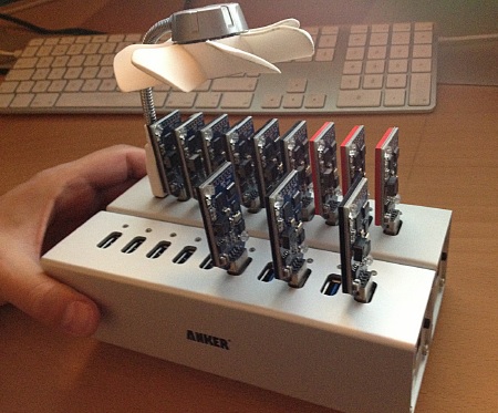
USB hub with a whole array of Block Erupters, each of which gives 330 MH / s or about half the performance of an AMD 7970 GPU. (Source)
Avalon
Another company that managed to attract investment through direct presales through the Internet. Her story is not so interesting, so I will not spend much time on it. ASICs manufactured by this company use 110nm TSMC process technology, each chip measuring 4x4 mm contains a single SHA256 conveyor, and the typical delivery consists of 300 chips mounted on the surface of three “blades” in a 4U form factor. Like ASICMINER, the company is located in China.
Initially, orders were placed on miners with a performance of 66GH / s @ 600W and a price of $ 1,299. Then came the miners in the format USB-stick. And now the company is developing ASIC on 55nm technology.
Bitcoin Hardware Scaling
To date, many mining enthusiasts have been able to pre-order miners, which will be manufactured using 28 or less nanometers technology. This raises a logical question - how bitcoin-miner chips are scaled in accordance with the technical process. Due to the problems of dark silicon, improvements in the performance of the next generation of microcircuits are limited to energy efficiency of ~ 1.4x for each step of the process. The logic of the Bitcoin miner is almost the worst case for dark silicon, even worse than Multicore or GPU, due to the almost complete absence of oncrystal memory and high activity of all circuit elements. Those. if, say, progress stops at 10nm, then only ~ 6.5x performance improvements can be expected, compared to 65nm chips. The story of when BFL had to reduce the frequency of its chips due to power consumption restrictions only once again shows what attempts to get out of the framework of “permitted” by dark silicon lead now.
After the rapid change of generations of miners passed to the transition to ASIC, the difference between subsequent generations of miners will not be so great as to quickly retire the old iron. There is a complete analogy with a PC - if in the mid-90s the productivity increase made the top-end iron into junk for 2-3 years, now the 5-year-old iron looks pretty good. For ASIC manufacturers, this will mean chasing energy efficiency, not productivity. And among the groups of enthusiasts for mining, the one who has access to the cheapest electricity will have the greatest benefit. There are already cases when old mining equipment was bought up and returned to service, say, near power plants, where electricity tariffs are much lower than urban ones.
Energy efficiency optimization
The 65nm chips from BFL consume ~ 5.5W per GH / s. For 130nm-ASICMINER and 110nm-Avalon chips, these figures are 8W and 9W, respectively. According to Dennard's law, when switching to 14nm, you can expect a 65/14 = 4.6x reduction in power consumption, approximately to the level of 1W per GH / s.
True, because The first generations of ASIC miners set themselves the goal of moving from FPGA to the ASIC era, then there is probably a huge scope for further optimization of the architecture and circuit design in order to reduce power consumption without degrading performance or increasing area. Among such optimizations may be the use of several voltage levels, the replacement of triggers for latches, or even the use of self-timed circuitry to save the energy that is spent on clocking. According to expert estimates, there is still at least a fourfold opportunity to reduce energy consumption within the process used.
In addition to the basic optimizations, there are many improvements that are typical of dark silicon, and for which the ASIC miner is great. For example, the use of voltage levels close to the threshold (NTV - Near Threshold Voltage). The absence of static memory and the need to transmit signals over a long distance inside the chip makes it possible to expect here another 5x lower energy consumption.
Also, since the hardware implementation of SHA256 is very simple, you can imagine a specialized manufacturing process for miners, by analogy with various processes used for memory and logic chips today.
Instead of conclusion
The development of bitcoin miners has led to the emergence of specialized solutions based on ASIC. Without any support from large companies. Users self-organized, themselves financed the development of software and hardware, overcame risks and mistrust, evaluated business plans and coped with the task of creating expensive chips with an incredibly small budget. This is an unheard of thing in our time, where the evaluation of efforts to create the latest generation of chips begins with a mark of $ 100 million, and the number of specialized chips falls from year to year.
What can be learned from this? Under what conditions is it really possible to create chips for a specific task? A few thoughts on this.
Custom-made chips are the most competitive compared to mass production, if they pass the “concentration test” - the benefit from using a specialized chip should be in itself and not in other components of the system. In the case of Bitcoin, profitability is a direct characteristic of the chip. Only a few additional factors, like electricity prices.
If the computations have high parallelism, and the specialized implementation is much less than the equivalent code for a general-purpose system, then ASIC is a good choice to make a performance leap.
Oddly enough, but studies conducted at universities have played a very modest role in the development of ASIC miners. There is an explanation for this. Firstly, university research is focused on the latest production technologies, which, due to their instability, are not suitable for quick use. Secondly, universities have free access to CAD systems worth tens of millions of dollars, licensed for non-commercial use only. This means that a university graduate simply doesn’t know how to make hardware cheap, without going broke on licenses.
Time to market is inversely proportional to the newness of the process used. 130nm will appear first, 65nm will appear later. In those cases where the use of ASIC does give a win, there is not much difference in the technical process used. But time is very important.
Investment capital also did not play a significant role. Largely due to the popular belief that “iron” startups are too expensive and take too much time. Users were able to finance the project themselves, even without resorting to the help of sites like kickstarter.
Bitcoin mining machines have a very strong and understandable explanation for people of their value - “you buy a miner and it brings you a lot of money”. In addition, this idea has already been tested on previous generations of miners.
Two of the development companies were from China and conducted their activities there. Although Silicon Valley is known to be at the forefront of progress, most of the work in small budgets is done in Asia. Cheap access to labor and licenses plays an important role. The design route used by ASICMINER in the United States would have cost $ 400K per license for each developer.
In order to achieve innovation in hardware, you need to try out a lot of new ideas, at low cost. But the modern semiconductor industry has moved away from this direction in the direction of expensive and very expensive chips. As a result, “semiconductor” startups are practically non-existent, and there are practically no areas where risky innovative ideas could be explored. Not because there are no ideas, but because it is very expensive. At the same time, the demand for hardware-engineers in the labor market is declining, and young specialists go to software companies for higher wages.
Source: https://habr.com/ru/post/205554/
All Articles