Simple SDR receiver on FPGA
In this article I will talk about how to make a fairly simple HF SDR receiver based on the DE0-nano debug card.
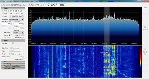
Example of received signals:
About SDR technology can be read here . In short, it is a method of receiving a radio signal, in which a large amount of information processing is performed in digital form. Through the use of FPGAs and high-speed ADCs, it is possible to make a receiver in which even the frequency transfer “down” is done digitally. This method is called DDC (Digital Down Conversion), you can read more about it here and here (more theory) . Using this technique, you can greatly simplify the receiver, in which the only analog part becomes the ADC.
And now more in detail about my receiver.
Its basis is the FPGA manufactured by Altera, installed on the debug board DE0-Nano. The fee is relatively cheap ($ 60 for students), but with rather expensive delivery ($ 50). Now it is becoming more and more popular among radio amateurs who are starting their acquaintance with FPGAs.
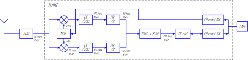
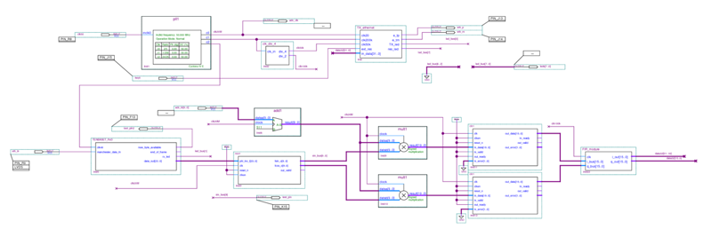
The main task of the FPGA is to “capture” the digital signal from the ADC, transfer it to the low-frequency range, filter and send the result to the computer. The block diagram of the receiver, implemented by me, has the following form:
')
Consider successively the components that the radio signal and digital information pass through.
Radio amateurs have a saying “A good antenna is the best amplifier.” Indeed, a lot depends on the antenna. Most of the most interesting short wave signals cannot be received on a simple antenna (for example, on a piece of wire). Outside the city there are no special problems - a rather long wire can work as a good antenna (at the reception). In the city, especially inside large reinforced concrete houses, things are much worse - a long antenna cannot be stretched, and there are a lot of disturbing noises (household appliances are capable of creating a very high noise level on the air), so choosing an antenna becomes difficult.
To receive radio signals, I use an active frame antenna, the design of which is described here .
My antenna looks like this:

In fact, the antenna is a large oscillating circuit (the capacitor is inside the box on the table). It is installed on the balcony, and works quite well. The main advantage of the frame antenna is that due to the use of the resonance phenomenon, it allows to suppress noise at unused frequencies, however there is a drawback: when switching from one frequency range to another, you need to rebuild.
Choosing an ADC is also not easy. The ADC must have a high bit depth to increase the dynamic range, and for the DDC receiver it must also have high speed. Usually, in good DDC receivers, they put an ADC with a 16-bit width and a speed of> 50 MSPS. However, the cost of such ADCs is more than $ 50, and I wanted to put something simpler into the experimental design.
I chose the AD9200 - 10-bit 20 MSPS ADC worth 200 rubles. These are very mediocre characteristics for a DDC receiver, however, as practice has shown, the ADC is quite suitable for receiving signals.
The ADC is installed on a separate board, which is inserted into the debug:
From the bottom, the board is metallized, the metal layer is connected to the ground by the ADC, which also protects from interference.
Since the ADC digitizes only the positive level signals, and the signal from the antenna is bipolar, the signal has to be shifted by half the reference voltage (for this are the resistors R1 and R2). The artificially created constant component is then subtracted from the digital signal in the FPGA.
All further signal processing after the ADC goes to the FPGA.
The data stream from the ADC is 200 Mbit (10-bit x 20 MSPS). To transfer such a stream directly to a computer, and then it is also very difficult to process it, so the signal frequency must be specifically reduced. When transferring to a lower frequency, the phenomenon of a “mirror channel” arises, to combat which quadrature frequency conversion is used — the signal is converted into a complex form (separation into two I / Q channels occurs). Transfer to a lower frequency is done by multiplying the original signal with the generator signal. The FPGA used has enough hardware multipliers, so this is not a problem.
In order to transfer the input signal to the desired frequency, it must be created. To do this, use the finished component Quartus - NCO (numerically controlled oscillator). The generator is supplied with a clock frequency that is the same as that of the ADC (20 MHz), the value determining the frequency is fed to its control input, and a digital sinusoidal signal of the desired frequency sampled at a frequency of 20 MHz is generated at its output. NCO is able to simultaneously generate a cosine signal, so that you can form a quadrature signal.
After mixing with the generator signal from the output of the multipliers, the signal comes out already transferred to a lower frequency, but still with a high sampling rate (20 MSPS). The signal needs to be decimated , that is, to discard some of the samples. It’s just not possible to discard the extra samples, as this will lead to a distortion of the output signal. Therefore, the signal must be passed through a special filter (CIC-filter). In this case, I wanted to get a 50 kHz signal sampling rate at the receiver output. It follows from this that the frequency should be lowered (20e6 / 50e3 = 400) times. Decimation will have to be done in 2 stages - first 200, then 2 times.
The first stage is exactly the CIC filter. I used a 5 cascade filter.
As a result of the operation, the CIC filter due to lowering the signal bandwidth of the output signal increases. With my receiver, I artificially limited it to 16 bits.
Since there are two channels in the receiver, two filters will also be required.
Unfortunately, the CIC filter has a rather steep frequency response tending to 0 when approaching the output sampling rate (100 kHz). To compensate for its curvature is the following filter.
This filter is needed in order to compensate for the decline in the frequency response of the CIC filter and perform another step of decimation (twice). Altera has already taken care of the method for calculating this filter - when creating a CIC filter, a program for Matlab is automatically generated; by running it, you can form coefficients for a compensation filter.
View the frequency response of the CIC, FIR and the resulting result (graphics builds the same program for Matlab):
It can be seen that at a frequency of 25 kHz, the CIC filter will attenuate the signal by 20 dB, which is very much, however, using the FIR filter, the attenuation is only 10 dB, and at lower frequencies there is practically no attenuation.
At the output of the FIR filter, taking into account decimation, the sampling frequency of the signal will be 50 kHz.
Why it was impossible to immediately decimate the signal 400 times? This is due to the fact that the cutoff frequency of the FIR filter must be 1/4 of its output. In this case, the sampling frequency at the output of the filter without decimation, as at its input, is 100 kHz. As a result, the cutoff frequency will be just 25 kHz, as can be seen in the graphs above.
Both filters are Quartus ready-made components.
The received data stream ((16 + 16) bit x 50 KSPS = 1.6 Mbit) needs to be transferred to the computer. I decided to transfer data via Ethernet. There is no such interface on the debug board. The most correct way would be to make a separate board with the PHY controller, run the Nios soft processor, and transfer data through them. However, this greatly complicates the design. I went a simpler way - Ethernet packets can be formed on the FPGA itself, so you can transfer data at a speed of 10 Mbit. In this case, the Ethernet cable is connected through an isolation transformer to the FPGA terminals. Projects with this principle of work can be found here and here .
As a basis, I chose the first project, partially completing it. In the initial project, the FPGA sends a specific UDP packet to the computer with the specified IP and MAC address. After conversion, the transmitter's Ethernet module could transfer 1024 bytes, reading them from the RAM. As a result, 256 pairs of 16-bit signal values taken from the filter outputs are sent to the computer in one packet. Since the data comes from the ADC continuously, and you need to send them to the computer as packets, you had to implement double buffering of memory - while one RAM is full, data from another RAM is transmitted via Ethernet. After the first RAM is full, both RAMs “swap”, for which a fairly simple control module is responsible.
Since at the output of the filters data is transmitted by a stream from a pair of 16 bit values, and separate bytes are transmitted via Ethernet, a module is introduced to convert the streams into the design, which converts a stream of 32 bits 50 KSPS to 8 bits 200 KSPS.
As it turned out, if you transmit a data stream at a speed of 1.6 Mbit, the device to which the receiver is connected does not even detect it (there is no link). This is due to the fact that data packets are transmitted with a period of about 5 ms, and in order to inform the other network device the connection speed (10 Mbit), it is necessary to transmit a special short pulse (NLP) every 8-24 ms. Due to the high frequency of packet transmission, the Ethernet module does not have time to transmit these pulses, and Autonegotiation does not occur.
Therefore, in order for the opposite device to still determine the connection speed, it is enough when turning on the receiver to temporarily reduce the packet transmission frequency (I have 4 times), thanks to which the Ethernet module manages to transmit NLP pulses.
In order to control the receiver (set the tuning frequency), a certain value must be passed to it, which will be used to set the NCO frequency.
To receive this value, the component from the above site, modified to receive data, and output them as a 24-bit number is also used. Since the receiver and transmitter modules are not connected with each other, ARP cannot be implemented, and in fact this means that the receiver will not have IP and MAC addresses. You can send information to it if you send a broadcast packet to the network.
Physically, as in the case of the transmitter, the power cord is connected to the debug board via a transformer. However, it is no longer possible to connect to arbitrary outputs of the FPGA, since the signal is quite small. You need to use pins that support the LVDS interface - it is differential.
Resources used by the FPGA program:
- 5006 LE
- 68 9-bit multipliers (64 of them are used in the FIR filter).
- 16,826 bit memory (8 M9K blocks).
View of the project in Quartus:
After the computer has received the data, they need to be processed. It is best to take the finished program. Usually, SDR programs implement the necessary digital filters, algorithms intended for the formation of sound and its filtering, the FFT of the received signal, the construction of its spectrum and the “waterfall”.
I use HDSDR and SDRSharp, they both support data entry using the same ExtIO libraries (Winrad program format). Library requirements are well documented .
Here is an example of creating such a library. I redid this example, added data from the network, gluing two packets together (the program takes at least 512 pairs of I / Q samples at a time), sending them to the program, and transmitting a broadcast packet with the calculated value for the NCO when changing the frequency in the program. Before that, I never had to create libraries, and in C ++ I am not strong, so the library can be written not at all optimally.
Since the sampling frequency of the I / Q signals at the output of the receiver filters is 50 kHz, the 50 kHz band will be available in the program for reception. (± 25 kHz from the frequency generated by the NCO).
The assembled receiver looks like this:
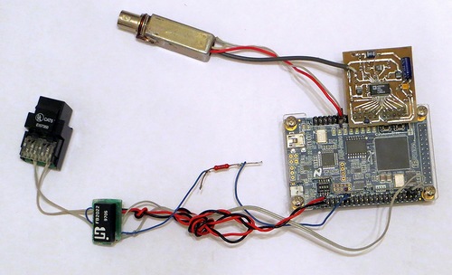
The resistor connects the middle points of the transformer to 3.3 V boards - this improves the reception and transmission of data over the network.
After the receiver was fully assembled and all programs were written, it turned out that there was not enough sensitivity. Even on an active antenna only broadcast radio stations and signals from radio amateurs operating at high power were received.
As I understand it, this is due to the low resolution of the ADC. To increase the sensitivity, we had to make an additional amplifier on the BF988 transistor (located inside a small metal box). The amplifier was able to significantly increase the sensitivity of the receiver.
Appearance of the whole structure:

The power supply unit provides a voltage of 12 V to power the antenna amplifier; in a metal round box there are several band-pass filters that reduce the out-of-band signals, which improves the example signals. I note that in many cases, reception is possible without DFT.
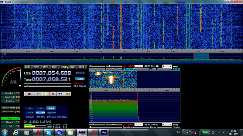
Now that manages to accept on KV. Despite the fairly high level of noise, it is possible to receive quite a lot of signals, broadcast stations are well received, and hams are well received.
An example of receiving signals in the HDSDR program (reception was conducted during the CQ WW DX Contest):
Reception video:
It is able to receive WSPRnet signals. WSPRnet is a network of amateur radio beacons that automatically exchange short messages with each other. Data from lighthouses is automatically published on the Internet. In this case, by installing a special program, you can decode the received signals and send them to the network. The site has the opportunity to look at the map, which shows the connection between the beacons for a certain period of time.
This is what happened in my half day reception:
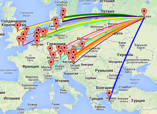
An important feature of WSPR is the very small transmitter power (less than 5 W), the narrow band of the transmitted signal, and the long duration for transmitting one message (2 minutes). Thanks to digital processing in the decoder program it is possible to receive very weak signals. I was able to receive a 100 mW beacon signal located at a distance of ~ 2000 km.
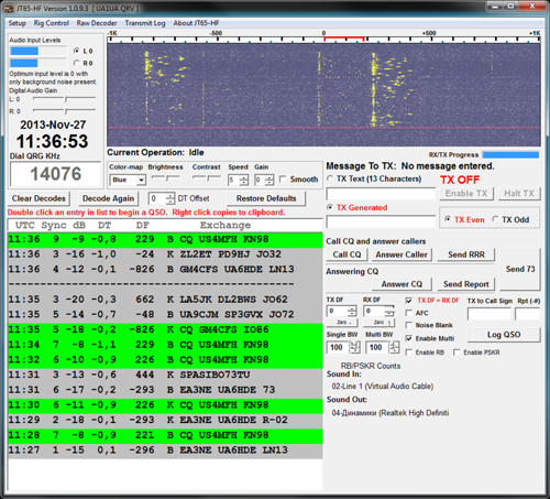
Hams using JT65. JT65 is one of the protocols of digital communication between radio amateurs. As in the WSPR, it uses small power and long-term transmission (1 min). Messages are received automatically, so you can leave the receiver for a long time, and then watch who you managed to receive.
Reception example:
Digital broadcasting (DRM). Some broadcast radio stations transmit sound in digital form. Accepting such signals is not easy in the conditions of the city - there is not enough signal level. It was possible to take one station:

There are many other radio signals that would be interesting to receive. There are weather weather faxes, RBU time station (at a strange frequency of 66.6 kHz), and others.
Project for Quartus + source code and ExtIO dll itself
Example of received signals:
About SDR technology can be read here . In short, it is a method of receiving a radio signal, in which a large amount of information processing is performed in digital form. Through the use of FPGAs and high-speed ADCs, it is possible to make a receiver in which even the frequency transfer “down” is done digitally. This method is called DDC (Digital Down Conversion), you can read more about it here and here (more theory) . Using this technique, you can greatly simplify the receiver, in which the only analog part becomes the ADC.
And now more in detail about my receiver.
Its basis is the FPGA manufactured by Altera, installed on the debug board DE0-Nano. The fee is relatively cheap ($ 60 for students), but with rather expensive delivery ($ 50). Now it is becoming more and more popular among radio amateurs who are starting their acquaintance with FPGAs.
The main task of the FPGA is to “capture” the digital signal from the ADC, transfer it to the low-frequency range, filter and send the result to the computer. The block diagram of the receiver, implemented by me, has the following form:
')
Consider successively the components that the radio signal and digital information pass through.
Antenna
Radio amateurs have a saying “A good antenna is the best amplifier.” Indeed, a lot depends on the antenna. Most of the most interesting short wave signals cannot be received on a simple antenna (for example, on a piece of wire). Outside the city there are no special problems - a rather long wire can work as a good antenna (at the reception). In the city, especially inside large reinforced concrete houses, things are much worse - a long antenna cannot be stretched, and there are a lot of disturbing noises (household appliances are capable of creating a very high noise level on the air), so choosing an antenna becomes difficult.
To receive radio signals, I use an active frame antenna, the design of which is described here .
My antenna looks like this:
In fact, the antenna is a large oscillating circuit (the capacitor is inside the box on the table). It is installed on the balcony, and works quite well. The main advantage of the frame antenna is that due to the use of the resonance phenomenon, it allows to suppress noise at unused frequencies, however there is a drawback: when switching from one frequency range to another, you need to rebuild.
ADC
Choosing an ADC is also not easy. The ADC must have a high bit depth to increase the dynamic range, and for the DDC receiver it must also have high speed. Usually, in good DDC receivers, they put an ADC with a 16-bit width and a speed of> 50 MSPS. However, the cost of such ADCs is more than $ 50, and I wanted to put something simpler into the experimental design.
I chose the AD9200 - 10-bit 20 MSPS ADC worth 200 rubles. These are very mediocre characteristics for a DDC receiver, however, as practice has shown, the ADC is quite suitable for receiving signals.
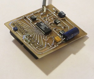
The ADC is installed on a separate board, which is inserted into the debug:
From the bottom, the board is metallized, the metal layer is connected to the ground by the ADC, which also protects from interference.
ADC connection diagram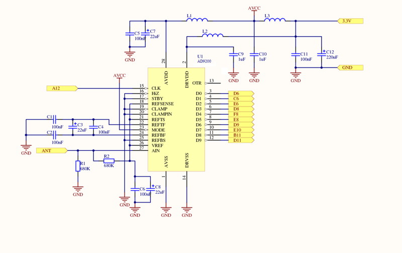
I have no experience in distributing RF designs, so it is possible that the layout and layout can be improved.
I have no experience in distributing RF designs, so it is possible that the layout and layout can be improved.
Since the ADC digitizes only the positive level signals, and the signal from the antenna is bipolar, the signal has to be shifted by half the reference voltage (for this are the resistors R1 and R2). The artificially created constant component is then subtracted from the digital signal in the FPGA.
All further signal processing after the ADC goes to the FPGA.
The data stream from the ADC is 200 Mbit (10-bit x 20 MSPS). To transfer such a stream directly to a computer, and then it is also very difficult to process it, so the signal frequency must be specifically reduced. When transferring to a lower frequency, the phenomenon of a “mirror channel” arises, to combat which quadrature frequency conversion is used — the signal is converted into a complex form (separation into two I / Q channels occurs). Transfer to a lower frequency is done by multiplying the original signal with the generator signal. The FPGA used has enough hardware multipliers, so this is not a problem.
NCO
In order to transfer the input signal to the desired frequency, it must be created. To do this, use the finished component Quartus - NCO (numerically controlled oscillator). The generator is supplied with a clock frequency that is the same as that of the ADC (20 MHz), the value determining the frequency is fed to its control input, and a digital sinusoidal signal of the desired frequency sampled at a frequency of 20 MHz is generated at its output. NCO is able to simultaneously generate a cosine signal, so that you can form a quadrature signal.
CIC filter
After mixing with the generator signal from the output of the multipliers, the signal comes out already transferred to a lower frequency, but still with a high sampling rate (20 MSPS). The signal needs to be decimated , that is, to discard some of the samples. It’s just not possible to discard the extra samples, as this will lead to a distortion of the output signal. Therefore, the signal must be passed through a special filter (CIC-filter). In this case, I wanted to get a 50 kHz signal sampling rate at the receiver output. It follows from this that the frequency should be lowered (20e6 / 50e3 = 400) times. Decimation will have to be done in 2 stages - first 200, then 2 times.
The first stage is exactly the CIC filter. I used a 5 cascade filter.
As a result of the operation, the CIC filter due to lowering the signal bandwidth of the output signal increases. With my receiver, I artificially limited it to 16 bits.
Since there are two channels in the receiver, two filters will also be required.
Unfortunately, the CIC filter has a rather steep frequency response tending to 0 when approaching the output sampling rate (100 kHz). To compensate for its curvature is the following filter.
FIR compensation filter
This filter is needed in order to compensate for the decline in the frequency response of the CIC filter and perform another step of decimation (twice). Altera has already taken care of the method for calculating this filter - when creating a CIC filter, a program for Matlab is automatically generated; by running it, you can form coefficients for a compensation filter.
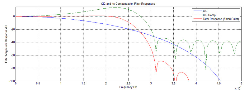
View the frequency response of the CIC, FIR and the resulting result (graphics builds the same program for Matlab):
It can be seen that at a frequency of 25 kHz, the CIC filter will attenuate the signal by 20 dB, which is very much, however, using the FIR filter, the attenuation is only 10 dB, and at lower frequencies there is practically no attenuation.
At the output of the FIR filter, taking into account decimation, the sampling frequency of the signal will be 50 kHz.
Why it was impossible to immediately decimate the signal 400 times? This is due to the fact that the cutoff frequency of the FIR filter must be 1/4 of its output. In this case, the sampling frequency at the output of the filter without decimation, as at its input, is 100 kHz. As a result, the cutoff frequency will be just 25 kHz, as can be seen in the graphs above.
Both filters are Quartus ready-made components.
Transfer data to computer
The received data stream ((16 + 16) bit x 50 KSPS = 1.6 Mbit) needs to be transferred to the computer. I decided to transfer data via Ethernet. There is no such interface on the debug board. The most correct way would be to make a separate board with the PHY controller, run the Nios soft processor, and transfer data through them. However, this greatly complicates the design. I went a simpler way - Ethernet packets can be formed on the FPGA itself, so you can transfer data at a speed of 10 Mbit. In this case, the Ethernet cable is connected through an isolation transformer to the FPGA terminals. Projects with this principle of work can be found here and here .
As a basis, I chose the first project, partially completing it. In the initial project, the FPGA sends a specific UDP packet to the computer with the specified IP and MAC address. After conversion, the transmitter's Ethernet module could transfer 1024 bytes, reading them from the RAM. As a result, 256 pairs of 16-bit signal values taken from the filter outputs are sent to the computer in one packet. Since the data comes from the ADC continuously, and you need to send them to the computer as packets, you had to implement double buffering of memory - while one RAM is full, data from another RAM is transmitted via Ethernet. After the first RAM is full, both RAMs “swap”, for which a fairly simple control module is responsible.
Since at the output of the filters data is transmitted by a stream from a pair of 16 bit values, and separate bytes are transmitted via Ethernet, a module is introduced to convert the streams into the design, which converts a stream of 32 bits 50 KSPS to 8 bits 200 KSPS.
As it turned out, if you transmit a data stream at a speed of 1.6 Mbit, the device to which the receiver is connected does not even detect it (there is no link). This is due to the fact that data packets are transmitted with a period of about 5 ms, and in order to inform the other network device the connection speed (10 Mbit), it is necessary to transmit a special short pulse (NLP) every 8-24 ms. Due to the high frequency of packet transmission, the Ethernet module does not have time to transmit these pulses, and Autonegotiation does not occur.
Therefore, in order for the opposite device to still determine the connection speed, it is enough when turning on the receiver to temporarily reduce the packet transmission frequency (I have 4 times), thanks to which the Ethernet module manages to transmit NLP pulses.
Receive data from a computer
In order to control the receiver (set the tuning frequency), a certain value must be passed to it, which will be used to set the NCO frequency.
To receive this value, the component from the above site, modified to receive data, and output them as a 24-bit number is also used. Since the receiver and transmitter modules are not connected with each other, ARP cannot be implemented, and in fact this means that the receiver will not have IP and MAC addresses. You can send information to it if you send a broadcast packet to the network.
Physically, as in the case of the transmitter, the power cord is connected to the debug board via a transformer. However, it is no longer possible to connect to arbitrary outputs of the FPGA, since the signal is quite small. You need to use pins that support the LVDS interface - it is differential.
Resources used by the FPGA program:
- 5006 LE
- 68 9-bit multipliers (64 of them are used in the FIR filter).
- 16,826 bit memory (8 M9K blocks).
View of the project in Quartus:
Computer data processing
After the computer has received the data, they need to be processed. It is best to take the finished program. Usually, SDR programs implement the necessary digital filters, algorithms intended for the formation of sound and its filtering, the FFT of the received signal, the construction of its spectrum and the “waterfall”.
I use HDSDR and SDRSharp, they both support data entry using the same ExtIO libraries (Winrad program format). Library requirements are well documented .
Here is an example of creating such a library. I redid this example, added data from the network, gluing two packets together (the program takes at least 512 pairs of I / Q samples at a time), sending them to the program, and transmitting a broadcast packet with the calculated value for the NCO when changing the frequency in the program. Before that, I never had to create libraries, and in C ++ I am not strong, so the library can be written not at all optimally.
Since the sampling frequency of the I / Q signals at the output of the receiver filters is 50 kHz, the 50 kHz band will be available in the program for reception. (± 25 kHz from the frequency generated by the NCO).
The assembled receiver looks like this:
The resistor connects the middle points of the transformer to 3.3 V boards - this improves the reception and transmission of data over the network.
After the receiver was fully assembled and all programs were written, it turned out that there was not enough sensitivity. Even on an active antenna only broadcast radio stations and signals from radio amateurs operating at high power were received.
As I understand it, this is due to the low resolution of the ADC. To increase the sensitivity, we had to make an additional amplifier on the BF988 transistor (located inside a small metal box). The amplifier was able to significantly increase the sensitivity of the receiver.
Appearance of the whole structure:
The power supply unit provides a voltage of 12 V to power the antenna amplifier; in a metal round box there are several band-pass filters that reduce the out-of-band signals, which improves the example signals. I note that in many cases, reception is possible without DFT.
Now that manages to accept on KV. Despite the fairly high level of noise, it is possible to receive quite a lot of signals, broadcast stations are well received, and hams are well received.
An example of receiving signals in the HDSDR program (reception was conducted during the CQ WW DX Contest):
Reception video:
It is able to receive WSPRnet signals. WSPRnet is a network of amateur radio beacons that automatically exchange short messages with each other. Data from lighthouses is automatically published on the Internet. In this case, by installing a special program, you can decode the received signals and send them to the network. The site has the opportunity to look at the map, which shows the connection between the beacons for a certain period of time.
This is what happened in my half day reception:
An important feature of WSPR is the very small transmitter power (less than 5 W), the narrow band of the transmitted signal, and the long duration for transmitting one message (2 minutes). Thanks to digital processing in the decoder program it is possible to receive very weak signals. I was able to receive a 100 mW beacon signal located at a distance of ~ 2000 km.
Hams using JT65. JT65 is one of the protocols of digital communication between radio amateurs. As in the WSPR, it uses small power and long-term transmission (1 min). Messages are received automatically, so you can leave the receiver for a long time, and then watch who you managed to receive.
Reception example:
Digital broadcasting (DRM). Some broadcast radio stations transmit sound in digital form. Accepting such signals is not easy in the conditions of the city - there is not enough signal level. It was possible to take one station:
There are many other radio signals that would be interesting to receive. There are weather weather faxes, RBU time station (at a strange frequency of 66.6 kHz), and others.
Project for Quartus + source code and ExtIO dll itself
Source: https://habr.com/ru/post/204310/
All Articles