Analysis of digital circuits for the risks of failure
Boolean algebra used to simulate the operation of digital circuits does not take into account the transition time (or inertia) of logical elements (for example, AND, OR) from one state to another (for example, from 0 to 1). In cases when the propagation time of a signal inside an element is sufficiently small, the transition delay can be ignored. But with an increase in the frequency of changes in input signals in real circuits, the effect of the propagation time of a signal inside its elements begins to have an effect. Such delays can cause unstable operation of devices (i.e., transitions that are not taken into account by the model, called failures , appear in the signals after successive passage through the nodes of the circuit). Many manufacturers of modern processors are kept secret, as they are struggling with failures caused by delays at frequencies on the order of GHz. After all, an ordinary conductor with a lot of close bends on the board in this mode of operation is already transformed into inductance.
To analyze the simplest schemes for the risks of failure, usually use the method of time diagrams, which has already become classical. The signals at each node are drawn strictly under each other; where necessary, an artificial delay in the transition from one state to another is made, and then output signals are built according to the boolean representation. This method is not good because it requires working with graphs, which may introduce an error in the received signals. And we need to know whether there will be a failure, and what it will look like.
In 2005, I touched on this topic and expressed my thoughts in this article in English. However, my good friend advised to write to Habrahabr for discussion with users.
')
In this topic, the procedure for analyzing schemas has been transferred from a graphical representation to a mathematical representation. At the same time, the parameter “time” is introduced into Boolean algebra by replacing logical operations with arithmetic ones. For ease of analysis, we consider asynchronous, i.e. unmanaged external (synchronizing or clocking) signal, digital circuits.
Let's start ...
Consider a numeric set . It identifies the operations of denial, conjunction, disjunction and produced from them (for example, implication, alternative disjunction, etc.). Express these logical operations in terms of arithmetic on the set M :
(one)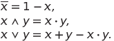
Show the validity of the law of de Morgan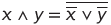 :
:

Add the rule to expressions (1)
(2)
for all natural values of m , the validity of which is obvious.
The expression for the Boolean function, which is a function of the input signals of the circuit, can now be simplified by the laws of arithmetic operations and rules (2). After simplifications go back to the boolean representation. At the same time, the minimization process itself can be automated by moving to symbolic calculations.
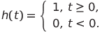
As you know, a single step function or Heaviside function is defined on the set of real numbers and returns the number belonging to the set M :
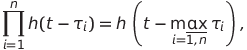
Let t be the current time. Note that the function h is also called the switching function. The following statement is obvious: any signal in the logic circuit, including the transition from one logical state to another, can be represented as a sum-difference of Heaviside functions, taken with the corresponding argument.
The obvious rule for the function h
(3)
Where - the point in time when the signal changes. Add rule (3) to (1) and (2).
Now, knowing the analytical expression for the input signals of the logic circuit, you can find the form of the function of the output signal.
The signal delay in a logic element is conveniently simulated as the difference between the argument of the Heaviside function and the delay duration (since for existing logic elements, the delay on the front (transition from 0 to 1) and decay (transition from 1 to 0) are approximately the same). Thus, any real logic element of the circuit can be modeled as a serial connection of the “pure” delay link for each input and an ideal logic element (here the delay is equal to the delay time). For example, the equation of the output signal of the conjunctor with a delay at the entrance has the form

Where and
and  - Functions describing the corresponding input signals.
The proposed algorithm for searching for faulty states is similar to the timing diagram method; the advantage of the method is that we do not work with graphic images of signals, but with their analytical expressions (with the possibility of an analytical assessment of the time characteristics of the failure):
1. Let the circuit under study function in accordance with a certain logical expression defined by DNF;
2. We define the functions of the input signals, which are transitions in the truth table, expressed through the Heaviside function;
3. Go along the path of the signals in the logic circuit in order to search for the expression for the output signal of the circuit, applying the rules (1) and (3);
4. If there is a difference of Heaviside functions in the resulting expression, then we have a static failure; if the Heaviside function with a delay argument is present, then the failure is dynamic.
Investigate the transition from set 1111 to set 1001 of the truth table for the circuit shown in Fig. one.
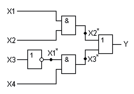
Fig. 1. Scheme that implements a Boolean function .
.
Imagine the input signals as follows (for simplicity, we will consider a change in state at a time instant equal to 5 time units):
Suppose that all elements have the same delays equal to . Then

Thus, we got a static failure — the resulting expression includes the difference of Heaviside functions (Fig. 2).

Fig. 2. Graph of signal Y ( t ).
In the topic was considered a method of analyzing digital circuits for the risks of failure, using an analytical representation of the signals inside the circuit. At the same time, the logical operations had to be replaced by arithmetic operations. Transitions from one signal state to another were described by the Heaviside function. The advantage of the described modification of the method of time diagrams is that there is the possibility of an analytical analysis of the characteristics of the failure.
To analyze the simplest schemes for the risks of failure, usually use the method of time diagrams, which has already become classical. The signals at each node are drawn strictly under each other; where necessary, an artificial delay in the transition from one state to another is made, and then output signals are built according to the boolean representation. This method is not good because it requires working with graphs, which may introduce an error in the received signals. And we need to know whether there will be a failure, and what it will look like.
In 2005, I touched on this topic and expressed my thoughts in this article in English. However, my good friend advised to write to Habrahabr for discussion with users.
')
In this topic, the procedure for analyzing schemas has been transferred from a graphical representation to a mathematical representation. At the same time, the parameter “time” is introduced into Boolean algebra by replacing logical operations with arithmetic ones. For ease of analysis, we consider asynchronous, i.e. unmanaged external (synchronizing or clocking) signal, digital circuits.
Let's start ...
1. The transition from the logical representation of Boolean functions to the arithmetic representation
Consider a numeric set
. It identifies the operations of denial, conjunction, disjunction and produced from them (for example, implication, alternative disjunction, etc.). Express these logical operations in terms of arithmetic on the set M :(one)
Show the validity of the law of de Morgan
:Add the rule to expressions (1)
(2)
for all natural values of m , the validity of which is obvious.
The expression for the Boolean function, which is a function of the input signals of the circuit, can now be simplified by the laws of arithmetic operations and rules (2). After simplifications go back to the boolean representation. At the same time, the minimization process itself can be automated by moving to symbolic calculations.
2. Input the time parameter into the Boolean algebra
As you know, a single step function or Heaviside function is defined on the set of real numbers and returns the number belonging to the set M :
Let t be the current time. Note that the function h is also called the switching function. The following statement is obvious: any signal in the logic circuit, including the transition from one logical state to another, can be represented as a sum-difference of Heaviside functions, taken with the corresponding argument.
The obvious rule for the function h
(3)
Where
- the point in time when the signal changes. Add rule (3) to (1) and (2).Now, knowing the analytical expression for the input signals of the logic circuit, you can find the form of the function of the output signal.
3. Delays in logic elements of the circuit
The signal delay in a logic element is conveniently simulated as the difference between the argument of the Heaviside function and the delay duration (since for existing logic elements, the delay on the front (transition from 0 to 1) and decay (transition from 1 to 0) are approximately the same). Thus, any real logic element of the circuit can be modeled as a serial connection of the “pure” delay link for each input and an ideal logic element (here the delay is equal to the delay time). For example, the equation of the output signal of the conjunctor with a delay
at the entrance has the formWhere
and - Functions describing the corresponding input signals.4. Algorithm for searching for failed states
The proposed algorithm for searching for faulty states is similar to the timing diagram method; the advantage of the method is that we do not work with graphic images of signals, but with their analytical expressions (with the possibility of an analytical assessment of the time characteristics of the failure):
1. Let the circuit under study function in accordance with a certain logical expression defined by DNF;
2. We define the functions of the input signals, which are transitions in the truth table, expressed through the Heaviside function;
3. Go along the path of the signals in the logic circuit in order to search for the expression for the output signal of the circuit, applying the rules (1) and (3);
4. If there is a difference of Heaviside functions in the resulting expression, then we have a static failure; if the Heaviside function with a delay argument is present, then the failure is dynamic.
5. An example of the analysis of the logical scheme.
Investigate the transition from set 1111 to set 1001 of the truth table for the circuit shown in Fig. one.
Fig. 1. Scheme that implements a Boolean function
.Imagine the input signals as follows (for simplicity, we will consider a change in state at a time instant equal to 5 time units):
Suppose that all elements have the same delays equal to
. ThenThus, we got a static failure — the resulting expression includes the difference of Heaviside functions (Fig. 2).
Fig. 2. Graph of signal Y ( t ).
Conclusion
In the topic was considered a method of analyzing digital circuits for the risks of failure, using an analytical representation of the signals inside the circuit. At the same time, the logical operations had to be replaced by arithmetic operations. Transitions from one signal state to another were described by the Heaviside function. The advantage of the described modification of the method of time diagrams is that there is the possibility of an analytical analysis of the characteristics of the failure.
Source: https://habr.com/ru/post/202052/
All Articles