IBM laboratories have learned how to get 10 centimeter sheets of graphene
Graphene is one of the most promising carbon-based materials. Thus, a transistor capable of operating at a frequency of 427 gigahertz, or a photosensor that is 1000 times more sensitive than usual can be made from graphene. Unfortunately, so far graphene can only be obtained in the form of scales the size of a fraction of a millimeter or in the form of films, though of a larger size, but consisting of several layers. At the same time, the cost of such graphene is still very high.
The IBM Research Center named after Thomas Watson has developed a technology for producing single-layer graphene sheets of up to 10 centimeters in size and applying them to a silicon substrate. This technology can be the basis for mass production of graphene and the appearance on the market of electronic devices based on it.
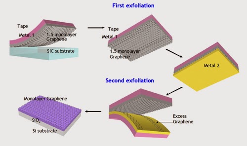
The essence of the new method of obtaining graphene is shown in the illustration and consists in using materials that “stick” to graphene with different strengths. First, a film with a thickness from one to several atomic layers of graphene is formed on the substrate of silicon carbide by the method of thermal decomposition. With the help of a thin film coated with nickel, graphene is detached from the substrate. This process was known before, but this graphene contained portions of several layers, which worsened its characteristics. The fact is that the uppermost surface layer is almost perfect, however, the “extra” pieces that form under the main sheet adhere to it.
')
IBM researchers added another step to the process — re-peeling the pieces of graphene adhering to the base layer. This is done with a gold-coated film. Graphene adheres to gold better than carbon, but worse than nickel. Due to this, it is possible to clean the graphene film from unnecessary pieces without damaging it, and transfer it to the silicon substrate. 99% of the surface of the resulting graphene sheet has an ideal structure. The process can be repeated again and again, separating the silicon carbide crystal layer by layer.
According to the Nature magazine's article on the prospects for graphene, modern silicon transistors will reach the theoretical limit of their capabilities already in 2021. The transition to graphene will open up a completely new era - the frequency of electronic devices can reach the terahertz.
The IBM Research Center named after Thomas Watson has developed a technology for producing single-layer graphene sheets of up to 10 centimeters in size and applying them to a silicon substrate. This technology can be the basis for mass production of graphene and the appearance on the market of electronic devices based on it.
The essence of the new method of obtaining graphene is shown in the illustration and consists in using materials that “stick” to graphene with different strengths. First, a film with a thickness from one to several atomic layers of graphene is formed on the substrate of silicon carbide by the method of thermal decomposition. With the help of a thin film coated with nickel, graphene is detached from the substrate. This process was known before, but this graphene contained portions of several layers, which worsened its characteristics. The fact is that the uppermost surface layer is almost perfect, however, the “extra” pieces that form under the main sheet adhere to it.
')
IBM researchers added another step to the process — re-peeling the pieces of graphene adhering to the base layer. This is done with a gold-coated film. Graphene adheres to gold better than carbon, but worse than nickel. Due to this, it is possible to clean the graphene film from unnecessary pieces without damaging it, and transfer it to the silicon substrate. 99% of the surface of the resulting graphene sheet has an ideal structure. The process can be repeated again and again, separating the silicon carbide crystal layer by layer.
According to the Nature magazine's article on the prospects for graphene, modern silicon transistors will reach the theoretical limit of their capabilities already in 2021. The transition to graphene will open up a completely new era - the frequency of electronic devices can reach the terahertz.
Source: https://habr.com/ru/post/201440/
All Articles