Lock-free data structures. The basics: where did the memory barriers go from?

As soon as I became interested in lock-free algorithms, the question began to torment me - where did the need for memory barriers come from, to “put things in order” in the code?
Of course, after reading a few thousand pages of manuals on a specific architecture, we will find the answer. But this answer will be suitable for this particular architecture. Is it common? In the end, we want our code to be portable. And the C ++ 11 memory model is not sharpened for a specific processor.
The most acceptable general answer was given to me by Mr. Paul McKenney in his 2010 article Memory Barriers: a Hardware View of Software Hackers . The value of his article is in general: he built some simplified abstract architecture, using which he examines what a memory barrier is and why it was introduced.
Generally, Paul McKenney is a famous person. He is a developer and active promoter of RCU technology, which is actively used in the Linux kernel, and also implemented in the latest version of libcds as another approach to safe memory release (in general, I would like to tell about RCU separately). Also participated in the work on the C ++ 11 memory model.
The article is big, I give only the first half translation. I allowed myself to add some comments, [which are highlighted in the text as follows] .
Memory Barriers: a Hardware View of Software Hackers
What prompted the CPU designers to introduce memory barriers and thereby impose a pig on the developers? The short answer is: reordering memory accesses allows for better performance, and memory barriers are needed to “restore order” in things like synchronization primitives [and lock-free algorithms, of course] , where the correctness of the primitive depends on the order of memory accesses.
A detailed answer requires a good understanding of how the CPU cache works, and what is required for its even better performance. Therefore, we further:
- consider the cache structure;
- we describe how the cache coherence protocol ensures the visibility of each memory cell for different processors;
- Consider how store buffers and invalidate queues help the cache achieve maximum performance.
We will see that memory barriers are a necessary evil that is required to achieve high performance and scalability. The root of this evil is the fact that the CPU is orders of magnitude faster than the memory and processor interface with memory.
Cache structure

Modern CPUs are much faster than memory subsystems. The 2006 sample processor could execute 10 instructions per nanosecond, but it took many tens of nanoseconds to extract data from main memory. This disproportion in speed (more than two orders of magnitude!) Led to multi-megabyte caches on modern processors. Caches belong to processors and, as a rule, the access time to them is several cycles.
Note
In fact, it’s common practice to have multiple cache levels. The smallest cache is closest to the processor and is available in one clock. The second level cache has an access time of about 10 cycles. The most productive processors have 3 and even 4 levels of caches.
The CPU exchanges data with the cache in blocks, called cache lines (cache line), the size of which is usually a power of two - from 16 to 256 bytes (depending on the CPU). When the processor first accesses the memory cell, the cell is not in the cache — this situation is called a miss (cache miss or, more precisely, “startup” or “warmup” cache miss). A slip means that the CPU must wait (stalled) for hundreds of cycles until the data has been retrieved from memory. Finally, the data will be loaded into the cache, and subsequent calls to this address will find the data in the cache, so that the CPU will run at full speed.
After some time, the cache is full, and misses will cause the data to be pushed out of the cache to give space to the new requested data. Such misses are called capacity miss. Moreover, preemption can occur even when the cache is not full, as it is organized in hardware in the form of a hash table with a fixed bucket size (or set , as its developers call CPU).
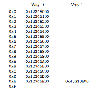
The figure on the right shows a 2-associative (2-way) cache with a 256-byte cache line. The line may be empty, which corresponds to an empty table cell. The numbers on the left are addresses whose data the cell may contain. Since the lines are aligned by 256 bytes, the lower 8 bits of the address are zero, and the hash function selects the next 4 bits as an index in the hash table. Suppose the program code is located at addresses 0x43210E00 - 0x43210EFF, and the program itself sequentially accesses data at addresses 0x12345000 - 0x12345EFF. Let now she addresses to the address 0x12345F00. This address is hashed to the 0xF line and both cells (ways) of this line are empty, so 256 bytes of data can be placed in one of them. If the program accesses the address 0x1233000, the hash of which is 0x0, then the corresponding 256-byte data can be placed in cell 1 (way 1) of the line 0x0. If the program accesses the address 0x1233E00 (hash = 0xE), then one of the lines (ways) must be pushed out of the cache in order to free up space for the new 256 bytes of data. If you later need access to this ejected data, we get a slip situation. Such a slip is called an associativity miss.
All this applies to reading data, and what will happen when writing? All CPUs must be matched according to data, so before writing, you must invalidate the data from the caches of other CPUs. Only after the invalidation is completed, can the processor safely write data. If the data is in the CPU cache, but is read-only, this is called write miss. Only after the CPU invalidates such data in the caches of other processors, the CPU can re-write (and read) this data. Further, if some CPU tries to access the data while the other CPU has invalidated them for recording, it will get a miss called communication miss , as this situation occurs when the data is used for interaction (communication), such as , mutex or spin-lock [means the mutex itself, not the data that it protects; A mutex is some kind of flag] .
As can be seen, great efforts must be made to manage the data coherence for all CPUs. With all this reading / invalidation / writing, it’s easy to imagine that the data will be lost or (worse,) different CPUs will have different data in their caches. These problems are solved by the data coherence protocol (cache-coherency protocol)
Cache coherency protocol
The protocol manages the state of the cache lines, ensuring integrity and prohibiting data loss. Such protocols can be very complex, with dozens of states, but for our purposes it is enough to consider the MESI protocol, which has 4 states.
MESI states
MESI is 4 possible states of the cache line: Modified-Exclusive-Shared-Invalid. To support this protocol, each line, in addition to the actual data, must have a two-bit tag that stores its state.
The Modified state means that the data in the cache lines has just been written by the processor-owner of the cache, and it is guaranteed that the change has not yet appeared in the caches of other CPUs. We can say that one CPU owns the data. Since the data in this line is the freshest, the cache line is ready to be written to memory (or to the next level cache), and the record must be made before the line can be filled with other data.
The Exclusive state is very similar to Modified, except that the data has not yet been altered by the cache-owning processor. This, in turn, means that the line contains the latest data consistent with the memory. The CPU owner can write to this cache line at any time without notifying other CPUs, as well as push it out without any entry back to memory.
The Shared state says that the line is duplicated in at least one other cache in another CPU. The CPU owner of such a line cannot write to it without prior approval from other CPUs. As for the Exclusive state, the line is consistent with memory, and can be pushed out without notifying other CPUs and without writing back to memory.
The cache line in the Invalid state is empty, that is, it does not contain any data (or contains garbage). When the cache needs to load new data, they are placed in the Invalid-line whenever possible.
Since all CPUs must maintain the coherence of the system caches in general, the protocol describes the messages by which the state changes of the cache lines of all processors are coordinated.
')
MESI protocol messages
Many of the transitions from one state to another require interaction between the CPUs. If all CPUs are connected to a single shared bus, the following messages are sufficient:
- Read : this message contains the physical address of the read cache line.
- Read Response : contains the data requested by the previous Read message. Read Response can come from a memory subsystem or from another cache. For example, if the data is already in a cache in the “modified” state, then such a cache may respond to Read
- Invalidate : contains the physical address of the cache line to be disabled. All other caches must delete the data and respond to this message.
- Invalidate Acknowledge : The CPU that received the Invalidate should delete the required data and acknowledge it with the Invalidate Acknowledge message.
- Read Invalidate : This message contains the physical address of the read cache line. At the same time, it dictates other caches to delete this data. In essence, this is a combination of the Read and Invalidate messages. This message requires a Read Response and Invalidate Acknowledgment response.
- Writeback : contains the address and the actual data to write to the memory. Allows caches to clear the corresponding line in the Modified state.
As you can see, a multiprocessor machine is a messaging system, essentially a computer under the processor cover.
Question answer
What happens if two processors invalidate the same cache line at the same time?
One of them (the “winner”) will access the shared bus first. Other CPUs must disable their copies of this cache line and respond with “invalidate acknowledge”. Of course, the “loser” of the CPU can immediately initiate the “read invalidate” transaction, so the win may be ephemeral.
If the message “invalidate” appears in a large multiprocessor system, all CPUs must answer “invalidate acknowledge”. Wouldn't the explosive stream of such responses lead to a complete stop of the system?
Yes, it can result if a large (large-scale) system is built this way. But systems such as, for example, NUMA, usually use the directory-based [directory in NUMA - node, node] protocol for supporting the coherence of caches just to prevent such cases.
MESI state diagram

Transitions in the figure on the right have the following meaning:
- Transition a (M -> E) : The cache line is written back into memory, but the CPU has left it in the cache and has the right to change it. This transition requires a “writeback” message.
- Transition b (E -> M) : CPU writes to the cache line, to which it has exclusive access. This transition does not require any messages.
- Jump c (M -> I) : The CPU receives a “read invalidate” cache line in the “Modified” state. The CPU must delete its local copy and respond with “read response” and “invalidate acknowledge” messages. Thus, the CPU sends data and shows that it no longer has a copy of it.
- Jump d (I -> M) : The CPU performs a read-modify-write (RMW) operation on data that is not in the cache. It issues a “read invalidate” signal, receiving data in a “read response”. The CPU completes the transition only when it receives all the “invalidate acknowledge” responses.
- Transfer e (S -> M) : The CPU performs a read-modify-write (RMW) operation on data that was read-only. It must initiate the “invalidate” signal and wait until it receives the full set of “invalidate acknowledge” responses.
- Transition f (M -> S) : Some other processor is reading data, and this data is in the cache of our CPU. As a result, the data becomes read-only, which can lead to writing to memory. This transition is initiated by the reception of the “read” signal. The CPU responds with a “read response” message containing the requested data.
- Transition g (E -> S) : Some other processor reads data, and this data is in the cache of our CPU. Data becomes shared and, therefore, read-only. The transition is initiated by the reception of the “read” signal. The CPU responds with a “read response” message containing the requested data.
- Transition h (S -> E) : The CPU decides that it needs to write data to the cache line, and therefore sends an “invalidate” message. The transition does not complete until the CPU receives the full set of invalidate acknowledge responses. Other CPUs flush the cache line with their “writeback” message, so our CPU becomes the only one caching this data.
- Transition i (E -> I) : Another CPU performs an RMW operation with data owned by our CPU, so our processor disables the cache line. The transition begins with the “read invalidate” message, our CPU responds with the “read response” and “invalidate acknowledge” messages.
- Jump j (I -> E) : The CPU saves the data to the new cache line and sends the “read invalidate” message. The CPU cannot complete the transition until it receives a “read response” and a full set of “invalidate acknowledge”. As soon as the recording is completed, the cache line goes to the “modified” state through the transition (b)
- Jump k (I -> S) : The CPU loads the data into the new cache line. The CPU sends a “read” message and completes the transition, receiving a “read response”
- Transition l (S -> I) : Another CPU wants to save data to the cache line, which has the status read-only, as some third CPU (or, for example, ours) shares the data with us. The transition begins by accepting “invalidate”, and our CPU responds with “invalidate acknowledge”
Question answer
How does iron handle such heavy transitions that require multiple delays?
Usually - the introduction of additional states. But such states do not need to be stored in cache lines, that is, they are not cache line states. At any given time, only a few cache lines can be in a transition state. It is the presence of heavy, time-distributed transitions that makes real cache coherence support protocols much more complicated than the simplified MESI described here.
Usually - the introduction of additional states. But such states do not need to be stored in cache lines, that is, they are not cache line states. At any given time, only a few cache lines can be in a transition state. It is the presence of heavy, time-distributed transitions that makes real cache coherence support protocols much more complicated than the simplified MESI described here.
MESI protocol example
Let's take a look at how MESI works in terms of the cache line, using the example of a 4-processor system with direct memory mapping to the cache. The data is in memory at address 0. The following table illustrates the change in data. The first column is the serial number of the operation, the second is the number of the processor performing the operation, the third is which operation is in progress, the next four columns are the cache line status of each CPU (in the form of memory address / state), the final two columns are whether the memory contains valid data (V) or not (i).

At first, the CPU cache lines are in the “invalid” state, and the memory contains valid data. When CPU 0 reads data at address 0, the CPU 0 cache line goes to the “shared” state and is aligned with the memory. CPU 3 also reads data at address 0, so that the cache lines go to the “shared” state in the caches of both CPUs, but are still consistent with the memory. Next, CPU 0 loads data at address 8, which leads to crowding out the cache line and placing new data into it (read at address 8). Next, CPU 2 reads data at address 0, but then realizes that it needs to write them (RMW operation), so it uses the “read invalidate” signal to make sure that it has an exclusive copy of the data. The “read invalidate” signal invalidates the cache line of CPU 3 (although its data is still consistent with the memory). Then, CPU 2 performs the recording, which is a part of the RMW operation, which switches the cache line to the “Modified” state. The data in memory is now obsolete. CPU 1 performs an atomic increment and uses the “read invalidate” signal to receive data. It receives data from the CPU 2 cache, and in the CPU 2 itself, the data is disabled. As a result, the data is located in the cache line of CPU 1 in the “modified” state and is still not consistent with the memory. Finally, CPU 1 reads data at address 8, which resets the cache line to memory (using the “writeback” message).
"Question answer"
The cache contains some data when we stopped our example. And what sequence of operations should be in order to switch the cache lines of all CPUs to the “invalidate” state?
Such a sequence does not exist, except that the CPU supports a special instruction to flush the cache (“flush my cache”). Most processors have such instructions.
Such a sequence does not exist, except that the CPU supports a special instruction to flush the cache (“flush my cache”). Most processors have such instructions.
Unwanted downtime during recording
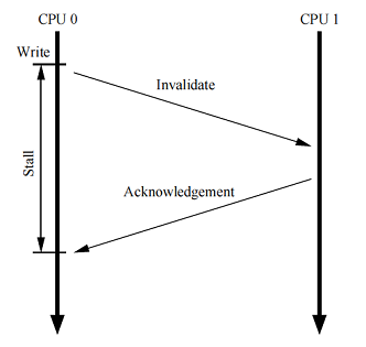
Although the cache structure we reviewed earlier provides good read / write performance for the CPU that owns this data, the performance of the first write to a specific cache line is very poor. To see this, consider the figure on the right.
The figure shows the write delay by processor 0 of the cache line, which is in the cache of CPU 1. CPU 0 must wait for a rather long period of time until the cache line becomes available for writing - it will transfer from the cache of CPU 1 to the CPU 0 ownership. The time required for transferring the cache line from one CPU to another, usually by orders of magnitude longer than the duration of the instruction working with registers.
But for CPU 0 there is no reason to wait that long: regardless of the data transmitted by CPU 1, CPU 0 will certainly overwrite it.
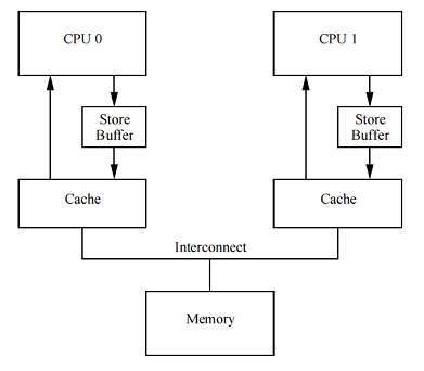
Store buffers
One method of dealing with unwanted downtime is to add a store buffer between each CPU and its cache, as shown in the figure to the right. With such a buffer, CPU 0 can simply write a write operation to its store buffer and continue working. After the necessary messaging, when the cache line finally transitions from CPU 1 to CPU 0, the data can be moved from the store buffer to the cache line of processor 0.
However, this solution leads to additional problems, which we will consider in the next two sections.
Store forwarding
To see the first problem, called self-consistency, consider the following code:
1 a = 1; 2 b = a + 1; 3 assert( b == 2 ); The variables “a” and “b” have an initial value of 0. The variable “a” is in the cache of processor 1, and the variable “b” is in the cache of processor 0.
It would seem, how can this
assert work at all? However, if someone implemented a processor with an architecture like the one in the figure, he would be surprised. Such a system could potentially produce the following sequence of events:- 1. CPU 0 starts performing
a = 1 - 2. CPU 0 looks to see if “a” is in its cache, and sees that it is not - miss
- 3. Therefore, CPU 0 sends a “read invalidate” signal to get exclusive rights to the cache line with “a”
- 4. CPU 0 writes “a” to its store buffer
- . CPU 1 receives a “read invalidate” message and responds to it by sending the cache line with “a” and invalidate its cache line
- 6. CPU 0 starts to execute
b = a + 1 - 7. CPU 0 receives a response from CPU 1, which still contains the old, zero value “a”, and places the line in its cache.
- 8. CPU 0 loads “a” from its cache - the value zero is loaded
- 9. CPU 0 executes the cache write request stored in the store buffer by writing the value “a” = 1 to the cache line.
- 10. CPU 0 adds one to zero, read earlier as “a”, and stores the result in the cache line “b” (which, as we remember, is in the possession of CPU 0)
- 11. CPU 0 executes
assert(b == 2)and gives an error -assertworks.
The problem is that we have two copies of “a” - one in the cache and the second in the store buffer.
This example violates a very important guarantee: each CPU must always perform operations in the order they are specified in the program (the so-called program order ). For programmers, this guarantee is an intuitive requirement, so hardware-engineers had to implement store forwarding : each CPU reads data not only from its cache, but also from the store buffer. In other words, each write operation can be directly transferred to the next read operation through the store buffer, without accessing the cache.
With store forwarding, step 8 in the above example should read the correct value 1 of the variable “a” from the store buffer. As a result, the value of “b” will be 2, which is what we need.
Write buffers and memory barriers
To see another problem, global memory order violation (global memory ordering), consider the following example, in which the variables “a” and “b” have an initial value of 0:
1 void foo() 2 { 3 a = 1; 4 b = 1; 5 } 6 7 void bar() 8 { 9 while ( b == 0 ) continue; 10 assert( a == 1 ); 11 } Let CPU 0 do
foo() , and CPU 1 do bar() . Suppose the memory containing “a” is only in the cache of CPU 1, and the CPU 0 owns the memory containing “b”. Then the following sequence of actions is possible:- 1. CPU 0 performs
a=1. The cache line for “a” is not in the cache of CPU 0, so CPU 0 places the new value “a” in its write buffer and issues a “read invalidate” signal. - 2. CPU 1 executes
while (b==0) continue, but “b” is not in its cache, so it sends a “read” message - 3. CPU 0 performs
b = 1. He already owns “b” in his cache, that is, the corresponding cache line is in the “exclusive” or “modified” state - so he has every right to keep the new value “b” in his cache, without telling anyone anything - 4. CPU 0 receives the “read” message and sends a cache line with the latest value “b” in response, simultaneously translating this line to the “shared” state in its cache
- 5. CPU 1 receives the cache line with “b” and places it in its cache.
- 6. CPU 1 can now complete the execution
while (b == 0) continue, since it sees thatb == 1, and proceed to the next instruction - 7. CPU 1 executes
assert(a == 1). Since CPU 1 works with the old value “a”, the condition is not met - 8. CPU 1 receives the “read invalidate” message and transfers the cache line with “a” to CPU 0, simultaneously invalidating this line in its cache. But too late
- 9. CPU 0 receives the cache line with “a” and writes from the buffer (flushes the store buffer to its cache)
Question answer
Why is CPU 0 in step 1 forced to send the message “read invalidate” and not just “invalidate”?
Because the cache line contains not only the value of the variable “a”. The size of the cache line is quite large.
Because the cache line contains not only the value of the variable “a”. The size of the cache line is quite large.
Hardware engineers cannot help in this case, since the processors do not know anything about the relationship of variables in the program. Therefore, engineers have introduced memory barrier instructions with which programmers can express such data links in a program. The program fragment should be changed as follows:
1 void foo() 2 { 3 a = 1; 4 smp_mb(); 5 b =1; 6 } 7 8 void bar() 9 { 10 while ( b == 0 ) continue; 11 assert( a == 1 ); 12 } The memory barrier
smp_mb() [this is a real function from the Linux kernel] tells the processor to reset the store buffer before making the next cache entry. The CPU can either just stop, waiting until its store buffer becomes empty, or it can use the store buffer for subsequent entries, until all the entries already in the store buffer are executed [thus some FIFO order is induced in the store buffer] .The sequence of the program with a memory barrier
- 1. CPU 0 performs
a=1. The cache line for “a” is not in the cache of CPU 0, so CPU 0 places the new value “a” in its write buffer and issues a “read invalidate” signal. - 2. CPU 1 executes
while (b==0) continue, but “b” is not in its cache, so it sends a “read” message - 3. CPU 0 executes
smp_mb()and marks all items in its store buffer (includinga = 1). - 4. CPU 0 performs
b = 1. He already owns “b” (that is, the corresponding cache line is in the “modified” or “exclusive” state), but there are marked elements in the recording buffer. Therefore, instead of writing the new “b” value to its cache, it places the “b” in its write buffer, but as an unmarked item - 5. CPU 0 receives a “read” message and transfers the cache line with the initial value “b” (= 0) to processor 1. It also changes the state of the cache line to “shared”.
- 6. CPU 1 receives the cache line with “b” and places it in its cache.
- 7. CPU 1 could now complete
while (b == 0) continue, but it sees thatb=0, so that it is forced to continue the cycle. The new “b” value is still hidden in the CPU 0 write buffer - 8. CPU 1 receives a “read invalidate” message and transfers the cache line with “a” to processor 0, invalidating its cache line.
- 9. CPU 0 receives a cache line with “a” and performs a previously buffered record, switching its cache line from “a” to the “modified” state.
- 10. Since the “a” record is the only item marked with the
smp_mb()) call, CPU 0 can also write “b”, but the cache line with “b” is in the “shared” state - 11. Therefore, CPU 0 sends an “invalidate” message to processor 1.
- 12. CPU 1 receives an “invalidate” signal, invalidates the cache line with “b” in its cache and sends an “acknowledgment” signal to processor 0
- 13. CPU 1 executes
while (b == 0) continue, but the cache line with “b” is not in the cache, so it sends a “read” message to the processor 0 - 14. CPU 0 receives an “acknowledgment” message and transfers the cache line from “b” to the “exclusive” state, then stores the “b” in the cache
- 15. CPU 0 receives the “read” signal and transfers the cache line with the “b” processor 1. Along the way, the cache line with the “b” is transferred to the “shared” state
- 16. CPU 1 receives a cache line with “b” and writes it to its cache.
- 17. CPU 1 can now complete execution
while (b == 0) continueand continue further - 18. CPU 1 executes
assert(a == 1), but the cache line with “a” is not in its cache. As soon as he gets the value “a” from CPU 0, he will be able to continue execution. The “a” value will be the freshest andassertwill not work.
As you can see, even intuitively simple things lead to many complex steps in silicon.
Unwanted downtime during a sequence of entries
Unfortunately, each write buffer should be relatively small. This means that if the CPU performs a large sequence of entries, it completely fills its store buffer (for example, if each entry leads to a miss). In this case, the CPU must wait until all invalidations are completed so that it can then flush its buffer to the cache and continue execution. The same situation may occur immediately after the memory barrier, when all subsequent write instructions must wait for the completion of invalidations, regardless of whether these entries lead to cache misses or not.
This situation can be disrupted if the “invalidate acknowledge” messages are processed faster. One way to achieve this is to enter an “invalidate” or “invalidate” queue for each CPU.
Invalididate queue
One of the reasons why invalidate acknowledgment messages is so slow is because the CPU must be sure that the corresponding cache line is indeed disabled. Such invalidation can be quite long if the cache is busy, for example, if the processor intensively reads / writes data that is all in the cache. In addition, in a short time interval, a whole stream of invalidation messages occurs, the CPU can not cope with them, which leads to idle rest of the CPUs.
However, the CPU does not need to disable the cache line before sending a confirmation. It can put an invalidate message in a queue, of course, with full understanding that this message will be processed before the processor sends other messages relating to this cache line.

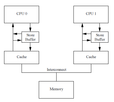
Invalidate Queues and proof of disability
The figure on the right shows the system with invalidate queues. A processor with an invalidate queue can acknowledge invalidate messages as soon as they appear in the queue, instead of waiting for the cache line to become invalid. Of course, the CPU must be consistent with its queue when it prepares to send an invalidate message: if the queue already contains an invalidation record for this cache line, the processor cannot immediately send its invalidate message. Instead, he must wait until the corresponding entry from the queue is processed.
Placing an item in the invalidate queue is essentially the processor’s promise to process this invalidate message before sending any MESI protocol signal related to a given cache line.
However, buffering invalidate signals leads to an additional possibility to disrupt the order of memory operations, as described below.
Invalidate queues and memory barriers
Suppose processors place invalidate requests in a queue and respond immediately. This approach minimizes the delay of cache invalidation, but may break the memory barrier, as we will see in the following example.
Let the variables “a” and “b” initially be zero and “a” be in the caches of both processors in the “shared” state (that is, read-only), and “b” is in the possession of CPU 0 (that is, the cache line in the “Exclusive” or “modified). Suppose CPU 0 performs
foo() , and CPU 1 performs bar() : 1 void foo() 2 { 3 a = 1; 4 smp_mb(); 5 b = 1; 6 } 7 8 void bar() 9 { 10 while (b == 0) continue; 11 assert(a == 1); 12 } The sequence of operations may be as follows:
- 1. CPU 0 performs
a=1. The corresponding cache line is read-only in the CPU 0 cache, so the processor places the new “a” value in its store buffer and sends the “invalidate” message so that the CPU 1 resets its cache line with “a” - 2. CPU 1 performs
while(b == 0) continue, but “b” is not in its cache. Therefore, it sends the message “read” - 3. CPU 1 receives “invalidate” from CPU 0, stores it in its invalidate queue and immediately responds
- 4. CPU 0 CPU 1,
smp_mb()( 4) “a” - 5. CPU 0
b=1. - “b”, “b” - 6. CPU 0 “read”- - “b” 1, “shared”
- 7. CPU 1 - “b”
- 8. CPU 1
while(b == 0) continue - 9. CPU 1
assert(a == 1). “a”,assert - , CPU 1 “invalidate”- - “a”
-
1 “invalidate”, “read invalidate”? , -?
CPU 0 , (shared) read-only - “a”. , CPU 0, , -. “invalidate”
CPU 0 , (shared) read-only - “a”. , CPU 0, , -. “invalidate”
So, in improving the speed of responses to disability there is little use if it leads to ignoring the memory barrier. Therefore, memory barriers must interact with the invalidate queue: when the processor executes the memory barrier, it must mark all elements in its invalidate queue and slow down all subsequent reads until the invalidate queue is completely processed by it.
Barriers to read and write
In previous chapters, memory barriers were used to mark items in the store buffer and invalidate queue. But in the last example, there are no reasons for
foo()interacting with the invalidate queue (since there is no read), as well as no reason for bar()interacting with the write buffer (because there is no record).Many architectures provide weaker (and, as a result, faster) memory barriers that allow you to streamline read only or write only. Roughly speaking, the read memory barrier only interacts with the invalidate queue (marks its elements, that is, it induces some order in the queue), and the write memory barrier only interacts with the store buffer (also marks its elements, brings order in the buffer). The full barrier interacts with both.
The effect of these semi-barriers is this: the reading barrier orders only the loads for the processor that performs the barrier. All readings before the barrier are completely completed, and only then do readings begin after the barrier. Similarly, a recording barrier orders only recording (stores) for its processor: all recordings up to the barrier are completed, and only then begin recording (stores) after the barrier. The full barrier organizes reads and writes, but again, only for the processor executing this barrier.
If we update our example so that
fooand barwill use the read / write barriers, we get the following: 1 void foo() 2 { 3 a = 1; 4 smp_wmb(); // 5 b = 1; 6 } 7 8 void bar() 9 { 10 while (b == 0) continue; 11 smp_rmb(); // 11 assert(a == 1); 12 } Some architectures have even a larger set of diverse barriers, but understanding the three options considered is enough to introduce memory barriers into the theory.

Translator's epilogue
This completes the translation. Further, the original is a brief overview of those barriers that provide modern architecture. I am referring to those interested in the original - in terms of volume, about the same remained there.
Let's take stock.
So, we have two operations of interaction of the processor with the cache / memory - read (load) and write (store). Two operations give us a total of four different memory barriers:
op1; // store load barrier ; // memory fence op2; // store load - Load / Load - orders the previous load-instructions with the subsequent. As we have seen, this barrier “brings order” to the invalidate queue: it either processes the queue entirely, or puts some labels in it that determine the order in which the queue is processed in the future. Relatively light barrier
- Store/Store – store- . store buffer: ( – ), , , - store buffer, - .
- Load/Store – load- store. ? , . ,
- Store / Load - organizes the previous store-instructions with subsequent load. Our store instructions go to the store buffer. That is, this barrier should be ordered by the store buffer - just put some tags in it? No, it seems that is not enough. After all, there is still speculative reading - this barrier should also be limited. On the basis of what I know about modern architectures, I can conclude that this barrier leads to the full processing of the store buffer, which is quite a heavy operation. Bottom line: this is the hardest barrier of all
Congratulations, we brought down the memory barriers of the Sparc architecture!
Sparc ( RMO – Relaxed Memory Ordering)
, Sparc :
, , —
Sparc ( RMO – Relaxed Memory Ordering)
membar , — , . — #LoadLoad , #LoadStore , #StoreStore , #StoreLoad ( , — ). membar , :Load1; membar #LoadLoad; Load2Load; membar #LoadStore; StoreStore; membar #StoreLoad; LoadStore1; membar #StoreStore; Store2
, Sparc :
membar #LoadLoad|#LoadStore|#StoreStore|#StoreLoad , , —
#StoreLoad . Sparc, weakly-ordered .Further
So, we looked at where the memory barriers come from. We learned that they are a necessary evil. We even tried to arrange them somehow in the code.
Displacing scheduler and memory barriers
, — ( , , Intel Itanium – load/store/RMW-). lock-free . /. , . ( ) . , – , ?
. - , , . lock-free , , , - .
. - , , . lock-free , , , - .
I would call the considered approach to the placement of memory barriers the read / wrire approach. During the development of the C ++ 11 standard, a read / write approach to the problems of streamlining memory access was considered too tied to the architecture and the acquire / release semantics was developed that formed the basis of the standard. As it was repeatedly stated in the article, the memory barriers directly affect only the processor that executes the barrier, and only indirectly (via the MESI protocol) - on other processors. The acquire / release model acts differently - it postulates how different parallel threads (ie, processors / cores) should interact , and almost nothing is said about how to achieve this. In fact, the implementation of this model is the use of certain memory barriers.
I am going to talk about the C ++ 11 memory model in the next article, Basics .
Source: https://habr.com/ru/post/196548/
All Articles