ARMs for the smallest
A couple of days ago I published and then suddenly removed an article on the plan in drafts to write about creating my own OS for ARM architecture. I did this because I received many interesting reviews both on Habré and in G +.
Today I will try to approach the question from the other side, I will talk about how to program ARM microcontrollers with examples of increasing complexity, until we write our OS or until I get bored. Or maybe we will jump to tinkering at Contiki, TinyOS, ChibiOS or FreeRTOS, who knows, there are so many different and interesting ones there (and TinyOS also has its own programming language!).
')
So why ARM? Although it is interesting to mess with 8-bit microcontrollers, it soon gets boring. In addition, ARM development tools run through a long experience and are much more pleasant to work with. At the same time, to start flashing the LEDs on some kind of “evaluation board” is as easy as on the Arduino.
A small excursion into architecture
ARM promotes a wonderful architecture, which it successfully licenses, it’s really hard for me to imagine which device has no presence of this company's products. Your smartphone is guaranteed to have several cores based on the ARM architecture. A couple more can be found in a modern laptop (and this is not even a CPU, but a companion controller of some peripherals), and a few more in the car. There are they in other household things: microwaves and televisions.
This flexibility is achieved by the fact that in the most basic version of the ARM core is very simple. Now there are three types of this architecture. Application is used in “general purpose” devices - as the main processor in a smartphone or netbook. This profile is the most feature-rich and functional, there is also a full-fledged MMU (memory management module), the ability to hardware-execute Java bytecode instructions and even support for DRM schemes. Microcontroller is the exact opposite of the application profile used (suddenly!) For use in microcontrollers. Here the actual power consumption and deterministic behavior. And, finally, real-time is used as an evolution of the microcontroller profile for tasks where it is critical to have a guaranteed response time. All these profiles have been implemented in one or more Cortex cores, for example, Cortex-A9 is based on the application profile and is part of the processor in the iPhone 4S, and Cortex-M0 is based on the microcontroller profile.
Pieces of iron!
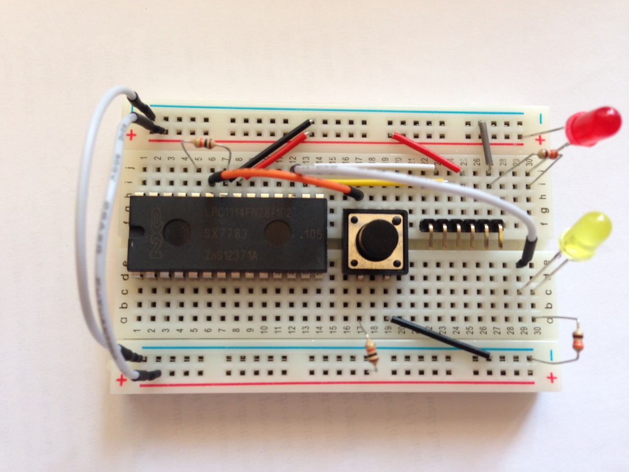
As a target platform, we will consider working with Cortex-M, since it is the simplest, respectively, we need to delve into fewer questions. As a test device, I suggest you LPC1114 - MCU manufactured by NXP, a circuit that can be assembled literally on the knee (no, really, you only need the MCU itself, a 3.3 V FTDI cable, several LEDs and resistors). The LPC1114 is based on the Cortex-M0, so this will be the most trimmed version of the platform.
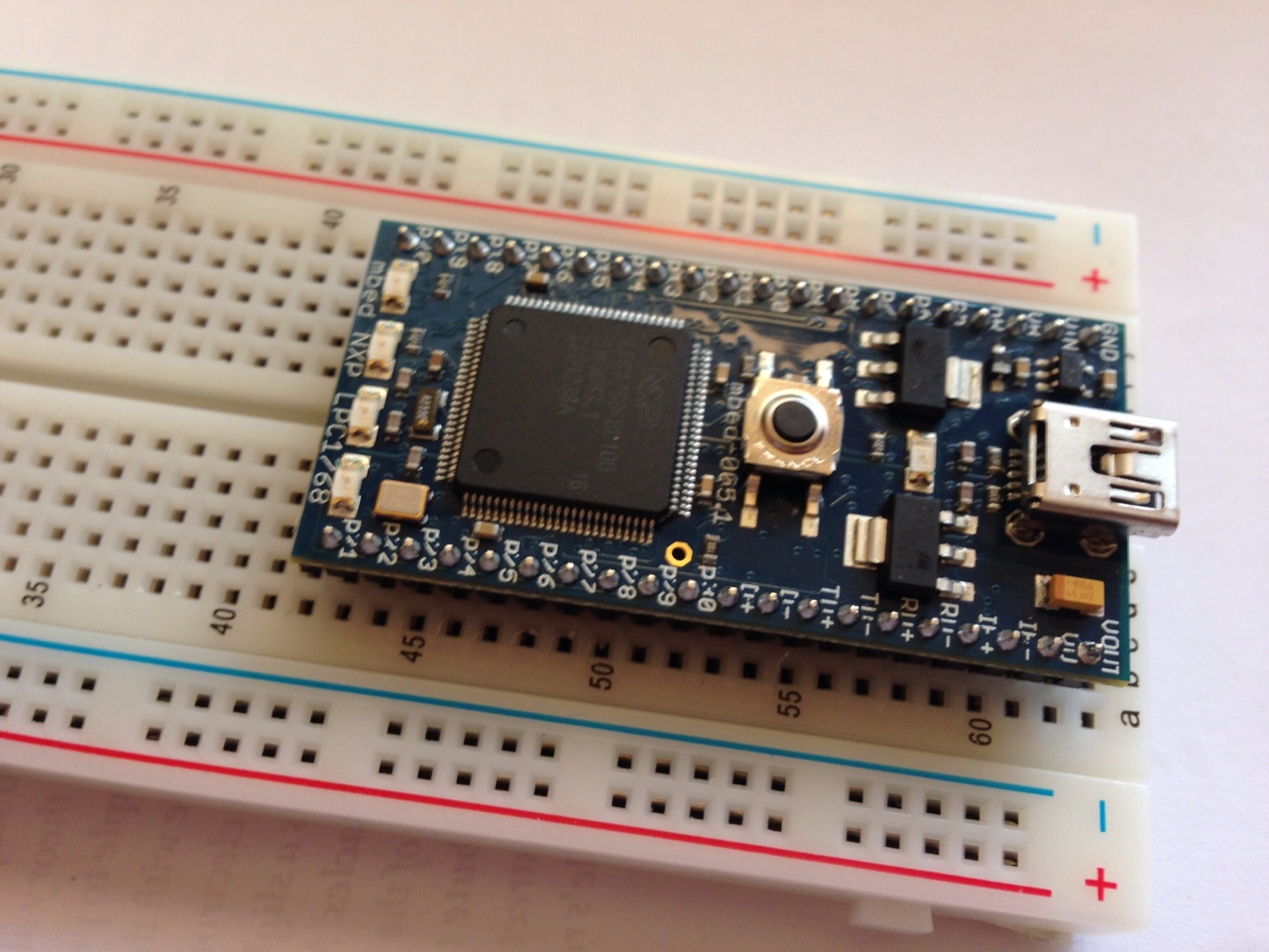
As an alternative, we will work with the mbed platform, and specifically, with the model based on LPC1768 (and therefore, inside there is a Cortex-M3, somewhat more sophisticated). The option is no longer so budgetary, but the process of pouring binaries onto a chip and debugging is simplified to the maximum. Yes, and you can play around with the mbed platform itself (in short: it’s an online IDE and a library with which you can program at the arduin level).
Let's get started
An interesting feature of modern ARMs is that they can be fully programmed entirely in C, without the use of assembler inserts (although the assembler is not so complicated, Cortex-M0 has only 56 commands). Although some commands are not available in principle from C, this problem is solved by CMSIS - Cortex Microcontroller Software Interface Standard. This is a driver for the processor that solves all the main tasks of managing it.
How does the processor load? A typical situation is when he just starts to execute commands from the address 0x00000000. In our case, the processor is somewhat smarter, and it relies on a specially-defined data format at the beginning of the memory, namely, the interrupt vector table:
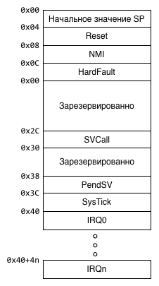
The program starts running as follows: the processor reads the value at 0x00000000 and writes it to SP ( SP is the register that points to the top of the stack), then reads the value at 0x00000004 and writes it to the PC ( PC is the register that indicates current instruction + 4 bytes). Thus, some user code starts to run, while we already have a stack pointing somewhere in memory (i.e., all the conditions for executing a program in C).
As a test exercise, we will flash the LED. We have four of them on the mbed, we install the LED into the circuit with LPC1114 (hereinafter referred to as the “board”) manually.
Before writing code directly, we need to figure out one more thing, namely, what should be located in memory. Since we do not work with some kind of "standard" OS, the compiler (or rather, the linker) cannot find out where it should have a stack, where the code itself is, and where it is a heap. Fortunately for us, the Cortex core family has a standardized memory card, which makes it relatively easy to port applications between different processors of this architecture. Work with the periphery, of course, remains processor-dependent.
The memory card for the Cortex-M0 looks like this:
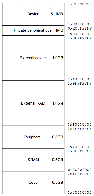
(image from Cortex ™ -M0 Devices Generic User Guide )
In Cortex-M3, it is, in fact, the same, but somewhat more detailed. The problem here is that NXP has its own, separate view on this issue, so we check the memory card in the processor documentation:
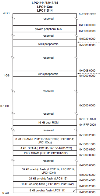
(image from LPC111x / LPC11Cxx User manual )
In fact, SRAM starts with 0x10000000! So, some standards, other standards, but still need to flip the volume of documentation.
Armed with this knowledge, let's go write code. First, the interrupt table:
.cpu cortex-m0 /* */ .thumb .word _stack_base /* , */ .word main /* Reset: */ .word hang /* NMI */ .word hang /* HardFault */ .word hang /* MemManage */ .word hang /* BusFault */ .word hang /* UsageFault */ .word _boot_checksum /* */ .word hang /* RESERVED */ .word hang /* RESERVED*/ .word hang /* RESERVED */ .word hang /* SVCall */ .word hang /* Debug Monitor */ .word hang /* RESERVED */ .word hang /* PendSV */ .word hang /* SysTick */ .word hang /* 0 */ /* ... */ /* 32 LPC1114 35 LPC1768, , */ .thumb_func hang: b . /* : */ .global hang Save this table in
boot.s Here, in fact, only one assembly insertion is the hang function, which arranges an infinite loop for the processor. All interrupts, except for reset, indicate it, so in the event of an unforeseen situation the processor will simply freeze, and it will not go to execute an incomprehensible piece of code.The table itself should be longer, but in fact we could finish it even after the Reset vector, the rest of us would not have worked in this example. But, just in case, we filled out the table almost entirely (except for user interrupts).
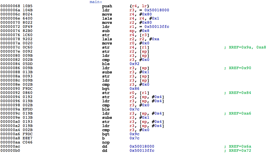
Now we will write the implementation of the main function:
#if defined(__ARM_ARCH_6M__) /* Cortex-M0 ARMv6-M, LPC1114 */ #define GPIO_DIR_REG 0x50018000 /* GPIO1DIR GPIO 1 */ #define GPIO_REG_VAL 0x50013FFC /* GPIO1DATA GPIO 1 */ #define GPIO_PIN_NO (1<<8) /* 8- 8- */ #elif defined(__ARM_ARCH_7M__) /* LPC1768 */ #define GPIO_DIR_REG 0x2009C020 /* FIO1DIR GPIO 1 */ #define GPIO_REG_VAL 0x2009C034 /* FIO1PIN GPIO 1 */ #define GPIO_PIN_NO (1<<18) /* 18- 18- */ #else #error Unknown architecture #endif void wait() { volatile int i=0x20000; while(i>0) { --i; } } void main() { *((volatile unsigned int *)GPIO_DIR_REG) = GPIO_PIN_NO; while(1) { *((volatile unsigned int *)GPIO_REG_VAL) = GPIO_PIN_NO; wait(); *((volatile unsigned int *)GPIO_REG_VAL) = 0; wait(); } /* main() ** ! */ } At mbed, the first LED is connected to the GPIO 1.18 port, on the board we connected the LED to GPIO 1.8. The same pins can perform different functions, these by default work exactly as GPIO (General Purpose I / O - general purpose input / output lines).
The code is relatively straightforward, if you keep on hand the LPC-shny User manual ( one and the second ). To begin with, we specify the GPIO mode through the GPIO_DIR_REG register (they are in different places for our processors, and in general LPC1768 can work more efficiently with GPIO), where 1 is the output, 0 is the input. Then we run an infinite loop, in which we write to the port alternately the values 0 and 1 (0 V and 3.3 V, respectively).
The function for “pause” works for us at random, simply scrolling through a relatively long cycle (
volatile int does not allow the compiler to optimize this cycle entirely).Finally, all this needs to be properly put together:
_stack_base = 0x10002000; _boot_checksum = 0 - (_stack_base + main + 1 + (hang + 1) * 5); MEMORY { rom(RX) : ORIGIN = 0x00000000, LENGTH = 0x8000 ram(WAIL) : ORIGIN = 0x10000000, LENGTH = 0x2000 } SECTIONS { .text : { *(.text*) } > rom .bss : { *(.bss*) } > ram } The linker script explains to him where we have a flash, where the RAM is, what sizes they have (here they use the sizes for LPC1114, since LPC1768 has the most, the shifts are, fortunately, identical). After determining the memory card, we indicate which segments to copy, .text (program code) gets into the flash, .bss (static variables that we don't have yet) - into memory. In addition, we specify two characters that were used in boot.s: _stack_base - points to the top of the stack and _boot_checksum (thanks to Zuy for the clarification!) - writes down the bootloader cheksum. Cheksumma is calculated using the following formula: additional code (2's compliment) on the sum of the fields above (i.e., the stack address, and all interrupts directly to the cheksum). Although the utilities for the firmware (see below) themselves would fix the checksum to the correct one, if we were to flash the code from the application itself, we would not be able to boot again.
Now we have three files: boot.s, main.c, mem.ld, it’s time to compile and finally run. As a toolchain, we will use GCC, later, perhaps, I will show how to do the same with LLVM. Users of OS X, I advise you to take the linchine from Linaro - at the very end of the list: Bare-Metal GCC ARM Embedded. I advise users of other operating systems to take the toolchain in the same place :-) (except that it will be easier for the gTushkens to crossdev and compile GCC).
arm-none-eabi-as boot.s -o boot.o arm-none-eabi-gcc -O2 -nostdlib -nostartfiles -ffreestanding -Wall -mthumb -mcpu=cortex-m0 -c main.c -o main-c0.o arm-none-eabi-gcc -O2 -nostdlib -nostartfiles -ffreestanding -Wall -mthumb -mcpu=cortex-m3 -c main.c -o main-c3.o arm-none-eabi-ld -o blink-c0.elf -T mem.ld boot.o main-c0.o arm-none-eabi-ld -o blink-c3.elf -T mem.ld boot.o main-c3.o arm-none-eabi-objdump -D blink-c0.elf > blink-c0.lst arm-none-eabi-objdump -D blink-c3.elf > blink-c3.lst arm-none-eabi-objcopy blink-c0.elf blink-c0.bin -O binary arm-none-eabi-objcopy blink-c3.elf blink-c3.bin -O binary An interesting point here is to disable the use of all standard libraries from GCC. Indeed, all the code that falls into the final binary is the code that we wrote ourselves.
Question: how does the linker know where to put the interrupt table? But he does not know, it is not written there :-). It simply links in succession, starting from the zero address, so the order of the files (boot.o, then main-c0.o) is very important! Try the opposite link or the boot.o link twice and compare the output in the lst file.
A good idea is to look at the final listing (lst file) or throw the binary into the disassembler. Even if you do not speak ARM UAL, then you can check visually that at least the interrupt table is in its place:
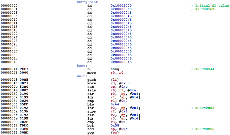
You can also pay attention to the funny moment - when compiling for Cortex-M3, GCC generates a wait () function more than in the version for Cortex-M0. True, if you turn on the optimization, it will set his brain.
Blink!
All that is left for us is to upload the binaries to our test platforms. With mbed, everything is as simple as possible, just copy
blink-c3.bin to a virtual USB flash drive and press reset (on mbed). With the board it's a little more complicated. First, in order to get into the bootloader, we need a resistor between GND and GPIO 0.1. Secondly, a program is needed for the firmware itself. You can use Flash Magic (Win, OS X), you can use the console utility - lpc21isp : lpc21isp.out -verify -bin /path/to/blink-c0.bin /dev/ftdi/tty/device 115200 12000 The firmware process is as follows:
- we put a resistor between j5 and j7 (10 kΩ will do);
- press reset;
- run lpc21isp;
- remove the resistor;
- Press reset again - the application is launched.
If you have the opportunity to run the examples on different devices, you will notice that the speed of flashing on them is not identical. This is due to the fact that different devices have different core frequencies, respectively, they perform
wait() at different times. In the next part, we will study the issues of oscillation in more detail and make a clear countdown.PS Special thanks to the pfactum habraiser for spending time correcting my mistakes in the text :-).
PPS Please those who have a test platform based on ARM - write in the comments - what. I can review the hardware base for further articles.
Source: https://habr.com/ru/post/189484/
All Articles