A brief excursion into the history of flash memory
We have already got used to taking many modern technologies for granted, not really thinking about how they work, what is behind them, what is the history of their development. This also applies to computers. I already wrote about the history of the development of data storage technologies , clearly showing the evolution in this industry. This time I decided to tell in more detail about one of the technologies actively used by LSI, about solid state, or SSD (Solid State Drive) memory.
It is used everywhere, starting with a chip that stores the computer's BIOS code (someone older - he remembers the Win.CIH virus, which disabled computers, erased the contents of this chip) and ending with state-of-the-art hybrid RAID controllers with a caching function, such as LSI Nytro, about which we told). Not to mention the different external drives, without which, perhaps, the progress of modern technology would be impossible: what anachronism the Sony Mavica MVC-FD5 digital cameras (and several other models), which saved images to 3.5 inch floppy disks, look like now.

The history of flash memory began in the middle of the 20th century, it was then, in the Arma division of American Bosch Arma Corporation, the ballistic scientist and digital computing pioneer Wen Tsing Chow worked to improve the memory blocks of the coordinates of the onboard computer of the Atlas E missile system / F. The solution he developed was secret for several years, since Atlas was armed with the American counterpart of the Strategic Missile Forces, but later the technology was declassified, and the technology called PROM (programmable read-only memory) became widespread.
')
The technology is rather simple in its essence: such a memory is the intersection of two arrays of conductors forming a coordinate grid. At the nodes of this grid, the conductors are closed by a special jumper. When it is necessary to determine the value of the cell by the given coordinates, it is sufficient to check whether the current passes through the intersection of the desired conductors. The presence of a current means that the jumper is intact, and corresponds to a value of 1, the opposite situation encodes 0. By default, all cells had the value 1. It is easy to guess that the programming of such microchips (called burning) was very simple: to those cells where zeros, high voltage applied, evaporating the jumper. Thus, the chips were obtained with the possibility of a one-time recording. In fact, it was possible to “add” the microcircuit, but only in the direction of erasing the jumpers. Also, due to the imperfection of technology, the jumper could recover, distorting the values. Checksums were used to combat data changes to both sides. In addition, the disadvantages of this type of microcircuit were a very small capacity.
But there were also PROMs (Russian translation of the abbreviation) and advantages: high speed of access to data and resistance to electromagnetic impulses, so valuable for places where nuclear explosions are not uncommon.
The next step in data storage technology was taken in the depths of Intel. Investigating the defects of microcircuits in which the transistor gates were destroyed, Dov Frohman-Bentchkowsky invented a new type of EPROM memory. Each cell of such a memory is a field-effect transistor with two gates: the first is the control one, the second is the floating one, which has no connection with other circuit elements. The insulation layer is a layer of silicon oxide.

To store the data, you need to select the desired cells and apply a higher voltage to them, this will allow electrons to pass through the insulation layer due to higher energy and accumulate on the gate (this tunneling effect is called Fowler-Nordheim). After the control voltage is removed, the electrons are "locked" at the gate, keeping the information for a long time. The main problem in this case is the inability to electrically erase information. To erase them use powerful ultraviolet lamps illuminating the chip through a special window made of quartz glass. The ultraviolet causes ionization in the insulating oxide layer, the charge leaks and the data is erased.
Such microcircuits were used as BIOS chips in old computers. The erase window is usually sealed with a sticker with the logo of the manufacturer to protect the chip from spontaneous erasure under the action of sunlight. Such chips, for example, were used in computers ZX Spectrum (Russian versions of the Search, Magic). It is these computers (many people remember the squeaky-modem sound made by cassette tapes with games recorded on them for these PCs) became for many modern engineers and specialists the first computers with which they started their way to IT.
In 1978, Intel's engineer George Perlegos presented the Intel 2816 chip, similar in technology to EPROM, but at the expense of a thinner layer of insulation, the chip could erase its contents without using ultraviolet radiation. This was the beginning of the EEPROM technology or in English EEPROM (Electrically Erasable Programmable Read-Only Memory). The main drawbacks of microcircuits made with this technology are the limited number of write cycles (although modern chips have brought this number to about a million) and spontaneous erasure of data (for current industrial-grade microcircuits, data storage is guaranteed for at least 3 years).
Since in the EEPROM chips for erasing it was necessary to create an electric field of high intensity in a sufficiently thin dielectric layer, this made it impossible to create rewritable memory chips with a high degree of arrangement. This, in turn, led to the development of two classes of devices: high-capacity, write-once microcircuits without erasability and rewritable chips of lower capacity. The problem was solved by Toshiba’s engineer Fujio Masuoka, the name given to his discovery was given by his colleague Shoji Ariizumi, who was reminded by the erasure of the erasing process. As it is not difficult to guess, they called these chips flash-memory (flash memory). The invention was presented to the public in 1984, and in 1988, Intel introduced commercial memory chips based on the NOR flash principle, and in 1989 Toshiba announced NAND memory.
As the memory elements, the same field-effect transistors with a floating gate are used in flash, while the voltage boost is used to erase and write, causing the tunneling effect already known to us. The main difference between flash microcircuits is that reading, writing and erasing are carried out by large blocks, while the recording block is no smaller than the reading block, and the erasing block is always larger than the recording block. This is due to the need to combine memory cells in a hierarchical structure, usually: blocks - sector - page.
Chips in which one cell stores one bit of information began to be called Single-Level Cell or SLC, and their alternative, in which each cell stores two bits of information due to the ability to store 4 charge levels, was called Multi-Level Cell or MLC. Thus, MLC chips are cheaper than SLC, but they are slower and less reliable. Recently, you can also see the abbreviation eMLC (Enterprise class MLC). This is usually denoted by devices that have increased read-write performance as well as increased service life compared to the MLC. Analyzing price characteristics, modern eMLCs cost about two times cheaper and only slightly inferior in speed and reliability to devices built on the basis of SLC.
The main difference between NOR and NAND is in the layout of the microcircuits. NOR uses a classic matrix of rows and columns with cells at the intersection, NAND is a three-dimensional array. In this case, you can greatly increase the layout area, but you have to “pay” for this by complicating the cell access algorithms. The access speeds are also different, for example, for NOR the read speed is tens of nanoseconds, for NAND - tens of microseconds.

The main field of application of NOR is a small-volume microcircuit, but with increased reliability requirements for storage: computer boot-up microchips, embedded memory of single-chip controllers, etc. NAND is the traditional data storage of the maximum amount: memory cards, SSD drives and so on. When using NAND, data storage redundancy and checksums are usually used to protect against failures. Also, microcircuits are usually equipped with “spare” blocks, which come into operation instead of those that have already “worn out”.
Modern flash drives are not possible without the use of service chips that control the storage of data on NAND chips. These chips are called FSP (Flash Storage Processor) or processors that control storage on flash memory. The company SandForce (now a division of LSI), is the leader in the production of this class of chips. Interestingly, the computational power of such processors is very, very high. The current generation incorporates 2 cores, has the ability to protect (with the calculation of verification amounts) data, similar to what we usually call RAID 50/60, and controls the digital garbage collection processes, monitors the uniform wear of memory cells, performs other service functions. With the introduction of such intelligent NAND memory management, modern devices have a predictable lifespan and programmable reliability. Having statistical data, it is very easy to make an SSD with the specified parameters of performance and reliability. Such service chips have long development cycles, and now they are developing chips that will work with flash memory chips, which will be made only in 2-3 years.

By the way, you can still find a fairly common misconception that when you reach the write limit, SSD devices die with data loss. This is not true. When certain limits on rewriting are reached, first the server administrator is sent warnings about the imminent service life of the device, and when the critical threshold is reached, the recording on the device stops, and the device itself goes into READ ONLY mode, only for reading. All modern storage controllers can work with this SSD functionality, and SSD users only need to purchase devices designed for their class of tasks. If this is a server, then you need to buy industrial-grade SSDs designed for 24x7 operation, if this is a laptop or desktop, cheaper devices will do.

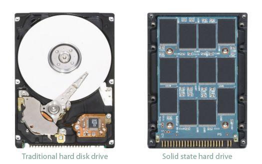
So, modern SSD or flash devices are presented today in the formats SD, USB-flash, SATA (SAS) SSD - in the same 2.5 ’’ and 3.5 ’’ form factors as HDD hard drives. In the server world, a PCIe-SSD is gaining momentum — a format where SSDs are mounted on a board that plugs directly into a PCI slot.
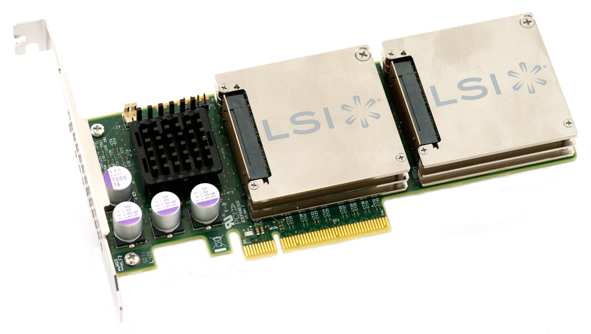 Nytro WarpDrive
For caching and diskless booting, SSDs are mounted on RAID controller cards.
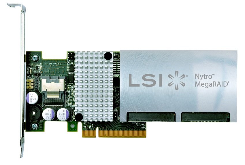 Nytro MegaRAID
External storage systems have been offering SSD instead of HDD for several years. In addition, there are special external data storage systems on flash technologies, for example, Violin and Ramsan.
Here is a brief insight into the history of flash memory. "Overboard" there are many interesting questions, starting with modern file systems, developed taking into account the features of flash memory, and ending with future developments that promise a lot of interesting things. Let's hope that you liked the story, and we will return to this topic in the future.
Based on personal experience, the internal resources of the company LSI (SandForce), resources of the Staff Staff, Wikipedia, courses MIT.
It is used everywhere, starting with a chip that stores the computer's BIOS code (someone older - he remembers the Win.CIH virus, which disabled computers, erased the contents of this chip) and ending with state-of-the-art hybrid RAID controllers with a caching function, such as LSI Nytro, about which we told). Not to mention the different external drives, without which, perhaps, the progress of modern technology would be impossible: what anachronism the Sony Mavica MVC-FD5 digital cameras (and several other models), which saved images to 3.5 inch floppy disks, look like now.
The history of flash memory began in the middle of the 20th century, it was then, in the Arma division of American Bosch Arma Corporation, the ballistic scientist and digital computing pioneer Wen Tsing Chow worked to improve the memory blocks of the coordinates of the onboard computer of the Atlas E missile system / F. The solution he developed was secret for several years, since Atlas was armed with the American counterpart of the Strategic Missile Forces, but later the technology was declassified, and the technology called PROM (programmable read-only memory) became widespread.
')
The technology is rather simple in its essence: such a memory is the intersection of two arrays of conductors forming a coordinate grid. At the nodes of this grid, the conductors are closed by a special jumper. When it is necessary to determine the value of the cell by the given coordinates, it is sufficient to check whether the current passes through the intersection of the desired conductors. The presence of a current means that the jumper is intact, and corresponds to a value of 1, the opposite situation encodes 0. By default, all cells had the value 1. It is easy to guess that the programming of such microchips (called burning) was very simple: to those cells where zeros, high voltage applied, evaporating the jumper. Thus, the chips were obtained with the possibility of a one-time recording. In fact, it was possible to “add” the microcircuit, but only in the direction of erasing the jumpers. Also, due to the imperfection of technology, the jumper could recover, distorting the values. Checksums were used to combat data changes to both sides. In addition, the disadvantages of this type of microcircuit were a very small capacity.
But there were also PROMs (Russian translation of the abbreviation) and advantages: high speed of access to data and resistance to electromagnetic impulses, so valuable for places where nuclear explosions are not uncommon.
The next step in data storage technology was taken in the depths of Intel. Investigating the defects of microcircuits in which the transistor gates were destroyed, Dov Frohman-Bentchkowsky invented a new type of EPROM memory. Each cell of such a memory is a field-effect transistor with two gates: the first is the control one, the second is the floating one, which has no connection with other circuit elements. The insulation layer is a layer of silicon oxide.
To store the data, you need to select the desired cells and apply a higher voltage to them, this will allow electrons to pass through the insulation layer due to higher energy and accumulate on the gate (this tunneling effect is called Fowler-Nordheim). After the control voltage is removed, the electrons are "locked" at the gate, keeping the information for a long time. The main problem in this case is the inability to electrically erase information. To erase them use powerful ultraviolet lamps illuminating the chip through a special window made of quartz glass. The ultraviolet causes ionization in the insulating oxide layer, the charge leaks and the data is erased.
Such microcircuits were used as BIOS chips in old computers. The erase window is usually sealed with a sticker with the logo of the manufacturer to protect the chip from spontaneous erasure under the action of sunlight. Such chips, for example, were used in computers ZX Spectrum (Russian versions of the Search, Magic). It is these computers (many people remember the squeaky-modem sound made by cassette tapes with games recorded on them for these PCs) became for many modern engineers and specialists the first computers with which they started their way to IT.
In 1978, Intel's engineer George Perlegos presented the Intel 2816 chip, similar in technology to EPROM, but at the expense of a thinner layer of insulation, the chip could erase its contents without using ultraviolet radiation. This was the beginning of the EEPROM technology or in English EEPROM (Electrically Erasable Programmable Read-Only Memory). The main drawbacks of microcircuits made with this technology are the limited number of write cycles (although modern chips have brought this number to about a million) and spontaneous erasure of data (for current industrial-grade microcircuits, data storage is guaranteed for at least 3 years).
Since in the EEPROM chips for erasing it was necessary to create an electric field of high intensity in a sufficiently thin dielectric layer, this made it impossible to create rewritable memory chips with a high degree of arrangement. This, in turn, led to the development of two classes of devices: high-capacity, write-once microcircuits without erasability and rewritable chips of lower capacity. The problem was solved by Toshiba’s engineer Fujio Masuoka, the name given to his discovery was given by his colleague Shoji Ariizumi, who was reminded by the erasure of the erasing process. As it is not difficult to guess, they called these chips flash-memory (flash memory). The invention was presented to the public in 1984, and in 1988, Intel introduced commercial memory chips based on the NOR flash principle, and in 1989 Toshiba announced NAND memory.
As the memory elements, the same field-effect transistors with a floating gate are used in flash, while the voltage boost is used to erase and write, causing the tunneling effect already known to us. The main difference between flash microcircuits is that reading, writing and erasing are carried out by large blocks, while the recording block is no smaller than the reading block, and the erasing block is always larger than the recording block. This is due to the need to combine memory cells in a hierarchical structure, usually: blocks - sector - page.
Chips in which one cell stores one bit of information began to be called Single-Level Cell or SLC, and their alternative, in which each cell stores two bits of information due to the ability to store 4 charge levels, was called Multi-Level Cell or MLC. Thus, MLC chips are cheaper than SLC, but they are slower and less reliable. Recently, you can also see the abbreviation eMLC (Enterprise class MLC). This is usually denoted by devices that have increased read-write performance as well as increased service life compared to the MLC. Analyzing price characteristics, modern eMLCs cost about two times cheaper and only slightly inferior in speed and reliability to devices built on the basis of SLC.
The main difference between NOR and NAND is in the layout of the microcircuits. NOR uses a classic matrix of rows and columns with cells at the intersection, NAND is a three-dimensional array. In this case, you can greatly increase the layout area, but you have to “pay” for this by complicating the cell access algorithms. The access speeds are also different, for example, for NOR the read speed is tens of nanoseconds, for NAND - tens of microseconds.
The main field of application of NOR is a small-volume microcircuit, but with increased reliability requirements for storage: computer boot-up microchips, embedded memory of single-chip controllers, etc. NAND is the traditional data storage of the maximum amount: memory cards, SSD drives and so on. When using NAND, data storage redundancy and checksums are usually used to protect against failures. Also, microcircuits are usually equipped with “spare” blocks, which come into operation instead of those that have already “worn out”.
Modern flash drives are not possible without the use of service chips that control the storage of data on NAND chips. These chips are called FSP (Flash Storage Processor) or processors that control storage on flash memory. The company SandForce (now a division of LSI), is the leader in the production of this class of chips. Interestingly, the computational power of such processors is very, very high. The current generation incorporates 2 cores, has the ability to protect (with the calculation of verification amounts) data, similar to what we usually call RAID 50/60, and controls the digital garbage collection processes, monitors the uniform wear of memory cells, performs other service functions. With the introduction of such intelligent NAND memory management, modern devices have a predictable lifespan and programmable reliability. Having statistical data, it is very easy to make an SSD with the specified parameters of performance and reliability. Such service chips have long development cycles, and now they are developing chips that will work with flash memory chips, which will be made only in 2-3 years.
By the way, you can still find a fairly common misconception that when you reach the write limit, SSD devices die with data loss. This is not true. When certain limits on rewriting are reached, first the server administrator is sent warnings about the imminent service life of the device, and when the critical threshold is reached, the recording on the device stops, and the device itself goes into READ ONLY mode, only for reading. All modern storage controllers can work with this SSD functionality, and SSD users only need to purchase devices designed for their class of tasks. If this is a server, then you need to buy industrial-grade SSDs designed for 24x7 operation, if this is a laptop or desktop, cheaper devices will do.
So, modern SSD or flash devices are presented today in the formats SD, USB-flash, SATA (SAS) SSD - in the same 2.5 ’’ and 3.5 ’’ form factors as HDD hard drives. In the server world, a PCIe-SSD is gaining momentum — a format where SSDs are mounted on a board that plugs directly into a PCI slot.
Nytro WarpDriveFor caching and diskless booting, SSDs are mounted on RAID controller cards.
Nytro MegaRAIDExternal storage systems have been offering SSD instead of HDD for several years. In addition, there are special external data storage systems on flash technologies, for example, Violin and Ramsan.
Here is a brief insight into the history of flash memory. "Overboard" there are many interesting questions, starting with modern file systems, developed taking into account the features of flash memory, and ending with future developments that promise a lot of interesting things. Let's hope that you liked the story, and we will return to this topic in the future.
Based on personal experience, the internal resources of the company LSI (SandForce), resources of the Staff Staff, Wikipedia, courses MIT.
Source: https://habr.com/ru/post/189294/
All Articles