Samsung introduced 3D-memory, Crossbar announced a breakthrough in RRAM
 On Monday, representatives of Samsung Electronics announced the start of production of three-dimensional vertical NAND chips. In the flash memory chips of a new type, thanks to the structure of silicon layers, the best performance is achieved in comparison with two-dimensional chips; According to the Korean company, the reliability will increase by 2-10 times, and the performance of the recording process will double. Thus, Samsung has become the first company in the world that launched the mass production of 3D NAND-memory chips.
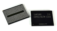
The new technology will be used in a wide range of tasks, including the creation of solid-state drives from 128 gigabytes to 1 terabyte. The longitudinal recording density of new microcircuits is 128 bits, and they are based on the bulk memory technology with a charge trap (3D Charge Trap Flash). The usual Charge Trap Flash was first introduced by Samsung back in 2006.
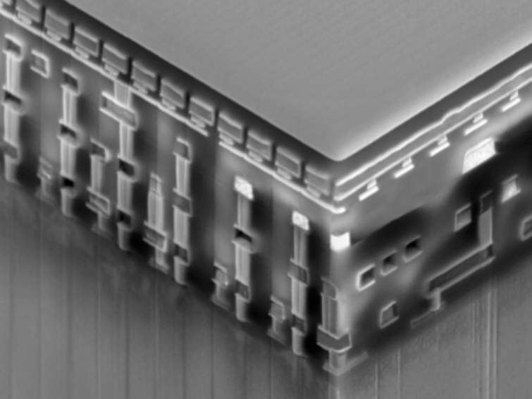
The number of vertical layers of microcircuits reaches 24, but their thickness is measured in nanometers, so thickening will not be noticeable even on a micrometer scale. Experts note that the limits of the number of layers are still unknown: today it is 24, there will be 32 in the next generation, and then this number will increase.
 The reasons for leaving to the volumetric layers are quite obvious: recently, flat scaling has become more and more complicated. With a decrease in the NAND chip process technology, the number of electron leaks increases, which creates data errors that can only be corrected by adding new, sophisticated error correction codes.
')
Bulk chips use old process technology of 40 and 50 nanometers. (For comparison: today, NAND-memory uses a process of about 20 nm.) This is due to the minimum thickness of the insulator between the layers, which also affects the performance and reliability. And the performance of the presented 3D-chips is still higher than that of a flat 10-nanometer NAND-memory.
The development of bulk chips has taken away from Samsung about 10 years, the company has made more than 300 patent applications worldwide. Representatives of the company are confident that the new technology opens the way to terabit NAND memory chips.
Currently, graphene-based microcircuits, phase change memory, Racetrack memory and resistive RAM are considered as a replacement for NAND flash memory. The latest type of memory promises to introduce the American Crossbar startup, according to the company , their RRAM chips will achieve a 20-fold superiority in writing speed over NAND memory, and the power consumption will be only a fraction of the usual flash memory requests.
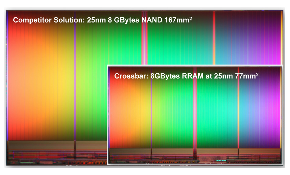
The company from the center of Silicon Valley - the city of Santa Clara - said that they managed to achieve a workable "simple and scalable" three-layer structure, so that using 3D technologies on a single chip the size of a postage stamp (200 mm²) will fit up to 1 terabyte information.
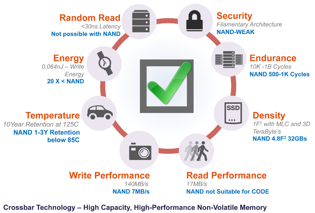
The promised superiority over today's NAND-flash limits is great: 20-fold reduction in power consumption, 20-fold increase in write speed, 10-fold increase in durability while reducing the size of the chip by half. Crossbar's memory chips will have the easiest integration into systems on a chip.
Investors did not ignore a promising startup: Crossbar received $ 25 million from the funds of Kleiner Perkins Caufield & Byers, Artiman Ventures and Northern Light Venture Capital. This was helped by the fact that the company had already managed to create a working prototype at the production facilities of one of its partners. Judging by at least three patents of the head of the company, Crossbar’s intentions are serious.
Like flash memory, RRAM is non-volatile, that is, information on it will not be reset even in the absence of power. According to the company's forecasts, the write speed will be 140 MB / s, the read speed is 17 MB / s with a random read delay of 30 nanoseconds. Three layers of chips consist of (from bottom to top) a non-metallic electrode at the bottom, a layer of amorphous silicon and a metal electrode.
Source: https://habr.com/ru/post/189250/
All Articles