Physics of radiation effects on electronics in space
Technological process with design standards of 32 nm.
Two 1.3 GHz ARMv7 cores
RAM - 1 GB.
Technological process with design standards 150 nm.
Single core PowerPC with a clock frequency of 200 MHz.
RAM - 256 MB.
Above - the parameters of the CPU iPhone5, below - the Curiosity rover. The on-board computer of the rover costs about two hundred times more than the new iPhone. Why is that? The central processor of the spacecraft is exposed to radiation. Habré already had a good overview article on space electronics, and I will try to tell you more about the physical principles and effects behind the failures and failures in space.
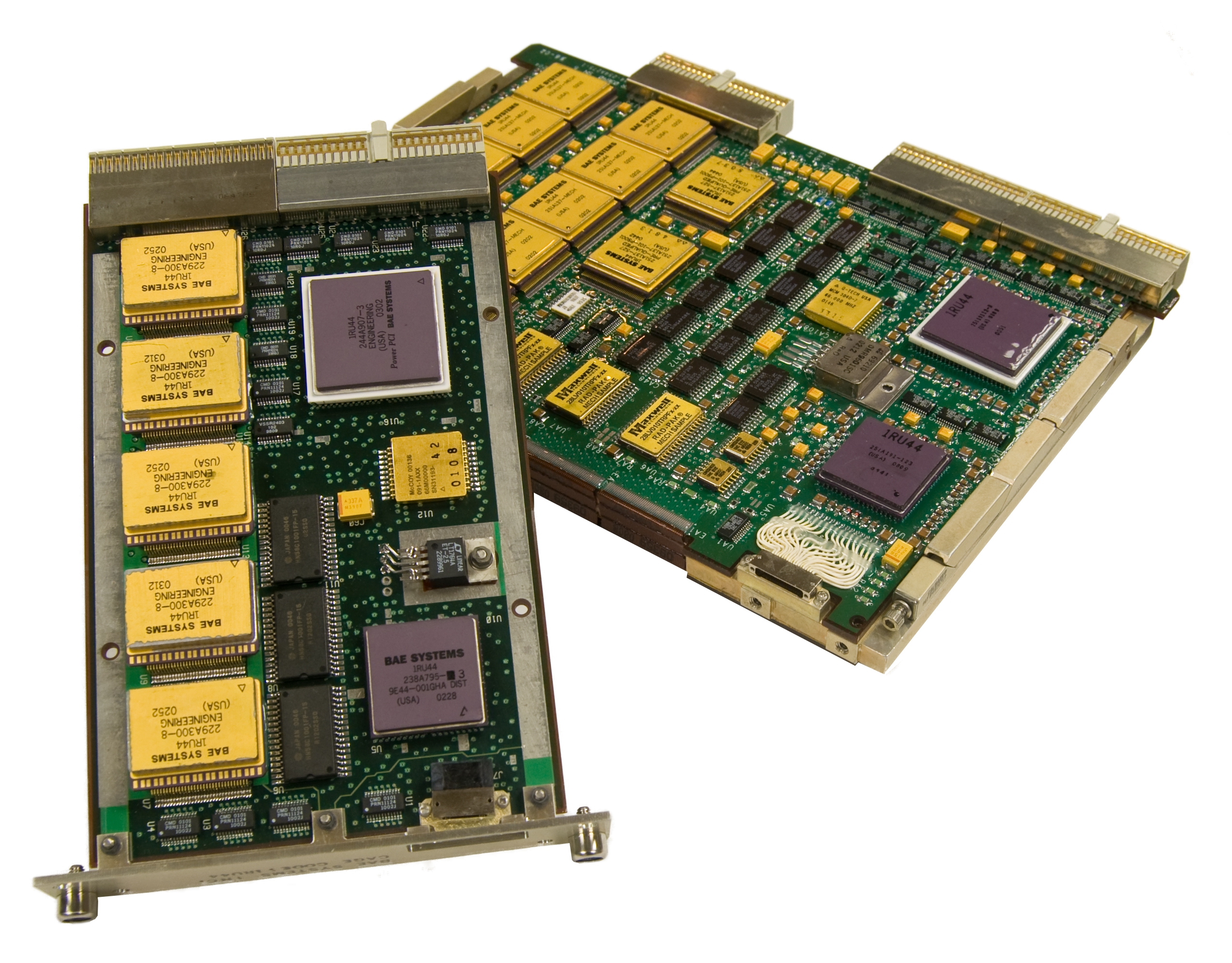
Figure 1. The cost of single-board computers RAD company BAE Systems is measured in hundreds of thousands of dollars.
')
The main sources of radiation are the sun and stars. Our own body supplies us with protons and electrons; from the rest of the stars everything flies, including, for example, the nuclei of heavy elements. The inhabitants of the Earth are protected from radiation by a magnetic field that collects particles flying into the radiation belts of the earth (also called van Allen belts). They are also a serious problem for spacecraft, so they try to minimize the time they spend in the radiation belts.
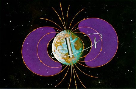
Figure 2. Earth's radiation belts.
What happens when a chip gets into space? There are two main effects - accumulation of the total absorbed dose (total ionizing dose, TID) and effects associated with exposure to single ionizing particles (Single Event Effects, SEE).
The total absorbed dose of radiation causes the drift of some characteristics of the chip, causing failures. The most important mechanisms vary from technology to technology; For modern microcircuits, radiation induced leakage currents are relevant, and in old technologies, the shift of the threshold voltage of the transistor played an important role.
Under the action of ionizing radiation, an electron-hole pair is formed in the microcircuit. Under normal conditions, these pairs quickly recombine (that is, a detached electron is captured by an atom back), but in an electric field, holes and electrons can separate (because the charges of opposite sign move in the field in different directions). The main insulator used in silicon chips is silicon dioxide (SiO 2 ). The mobility of electrons and holes in SiO 2 differs by several orders of magnitude; therefore, electrons are rapidly removed by silicon, and holes can accumulate in the oxide, and especially at the oxide – silicon interface.
If the charge has accumulated in the gate dielectric of the MOSFET, it will affect its operation as an additionally applied positive voltage (or as a threshold voltage shift). As a result, the n-channel transistor will be constantly ajar. In older technologies with thick gate dielectrics, the shift of the threshold voltage of n-channel transistors could be large enough for the transistor to completely stop closing, which naturally led to a loss of circuit performance. However, reducing the threshold voltage even earlier led to the fact that the total current consumption of the chip exceeded the permissible level due to leakage.
In modern technology, the thickness of the gate dielectric is a few nanometers, and they simply cannot accumulate enough holes for the threshold voltage of the transistor to seriously change. Therefore, the determining role is played by charge accumulation in other oxides present in the chip, namely, in the side insulation separating neighboring transistors, and at its boundary in the gate dielectric. The figure shows the cross section of the MOS transistor along the gate. The light layer is silicon, the dark one is SiO 2 . It is clearly seen that the side insulation is much thicker than the gate dielectric. The difference between pictures (a) and (b) is associated with various methods of making insulation and plays an important role in the radiation resistance of the transistor.
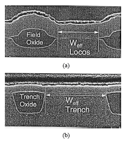
Figure 3. Section MOS structures with side insulation type LOCOS and STI.
In a thick insulating dielectric, the electric field is very small, and the separation of electron-hole pairs proceeds poorly. The field dielectric field is large, but the oxide itself is thin. But in the transition region, everything is good (that is, everything is bad) - the oxide is thick enough to accumulate charge in it, and the electric field is large enough that the holes and electrons are effectively separated.
The transistor in the microcircuit can be represented as a superposition of the actual transistor and two lateral parasitic transistors, in which the transition layer between the gate dielectric of the main transistor and the side insulation plays the role of a gate dielectric. The threshold voltage of the main transistor under the influence of the radiation dose varies little, but the threshold of parasitic structures can be reduced to zero, creating current flow channels not controlled by the gate. Through these channels, the current flows freely from the drain to the source — this is called the leakage current.
Leaks, as I said above, lead to an increase in the current consumption of the circuit (which may be unacceptable in a spacecraft, where the available power is very modest) and even to functional failures. For example, the most common problem with flash memory is not associated with storage elements, but with a high voltage generator used for rewriting. There are keys in this generator that, due to leaks, stop closing completely, without which it is impossible to form a voltage sufficient to overwrite the memory.
Single effects occur when a single ionizing particle (proton, neutron or nucleus of a heavier element) enters the transistor and is divided into “soft” (malfunctions) and “hard” (failures). The latter are quite a rare phenomenon characteristic of powerful circuits and poorly understood. Failure options include breakdown of the gate dielectric and burnout of the transistor due to the occurrence of the conducting channel between the drain and the source, as well as the thyristor effect, which I will dwell on in more detail later.
Soft failures have two main mechanisms — primary and secondary ionization. The first is characteristic of heavy charged particles (HTS; in this context they call all nuclei heavier than a proton), the second is for protons and neutrons. Flying through the microcircuit, the particle is inhibited due to the interaction with the crystal lattice and gives it some of its energy (this process can be compared with heating by friction).
The energy released during the passage of a particle ionizes the silicon atoms. Under normal conditions, the overwhelming majority of electrons torn from atoms come back, but if ionization occurs near a strong electric field, it can separate electrons and holes. The mechanism is similar to what happens with dose accumulation, but charge carriers cannot accumulate in silicon, and the duration of single effects is not measured in months, but in picoseconds.
A strong electric field in silicon is the source pn junction of a closed transistor, the separation of a charge near which leads to the fact that charge carriers of one sign fall into the ground / power line, and the second to the drain of the transistor. From the point of view of an external observer, the result of the process looks like a current pulse with a leading edge of several tens of picoseconds and a rear edge of several hundreds. The exact parameters of the pulse depend on many factors, including the technology of making the chip, the angle of incidence of the particle, etc.
If we integrate the resulting current pulse over time, we will get the full charge that is released as a result of the drop in the TZCH. The minimum charge leading to a failure is called the critical charge. The critical charge depends on the parameters of both the affected circuit and the incident particle; In addition, it is very difficult to measure experimentally, so it is usually used to simulate the interaction of a circuit and a particle and for comparative simulation of the failure resistance of different circuits.
Energy release is usually expressed using linear energy transfer (LET; the English term is Linear Energy Transfer, LET), measured in MeV × cm 2 / mg or more precisely, in (MeV / (mg / cm 3 )) / cm. One LET unit is the amount of energy emitted by a flying particle per centimeter of flying distance per unit density of the substance through which the particle flies. The definition at first glance is very confusing, but the unit of measurement chosen in this way has several important advantages: first, the numerical value is relatively easy to measure experimentally; secondly, thirdly, the values used in practice usually fall within the range from one to hundred.
LET - the value is not constant, that is, the parameters of the particle flying at the chip case cover, at the crystal boundary and directly at the transistor, under the numerous layers will be different. From this, however, it does not follow that a thicker body can help - the dependence of LET on the distance traveled in silicon usually has a maximum at a certain depth (the so-called Bragg peak). A similar effect is used in radiation therapy and in some operations for the manufacture of microcircuits: the parameters of implantable ions are chosen so that they stop at a certain depth and create a layer with a high doping level at depth.
Protons and neutrons have very small LET (approximately 0.01 MeV × cm 2 / mg), however, when a high-energy proton / neutron passes through silicon, there is a possibility of a nuclear reaction, the products of which are ions with a short mileage but a large LET (up to 15 MeV × cm 2 / mg). In technological processes with not aluminum, but copper metallization (180 nm and below), moreover, mechanisms of interaction of protons with tungsten, used for contacts of the first level (and located, thus, directly above sensitive pn junctions) are described. LET products of such reactions can reach 30 MeV × cm 2 / mg.
Typical minimum LET of incident particles, resulting in failure - within a dozen for technologies with design standards of 500-250 nm, and about one unit for sub-100 nm technologies, in which the critical charge can be so small that even primary ionization from protons and neutrons can cause a crash. In addition, a small critical charge failure leads to the fact that a sufficient charge can separate when a particle passes not only through the reverse-shifted stock pn-transition, but also through an unbiased source one, which significantly increases the vulnerable area on the crystal.
A short current pulse is perceived by the microcircuit as a pulse noise, and if its amplitude is sufficiently large, it can lead to switching of the element behind the affected transistor - this is a radiation-induced failure. Combination and analog circuits at the time of passage of a current pulse produces an incorrect result, and the storage elements are switched for good. Thus, the most vulnerable part of the microprocessor is the cache memory: there is a lot of it on the chip, and failures in it do not pass by themselves.

Figure 4. Diagram of a six-transistor storage element.
For example, it is most convenient to describe the failure mechanism in a six-transistor static memory cell (the simplest used storage element). The storage element consists of two inverters connected by positive feedback (M1-M2 and M3-M4) and two keys (M5-M6). In the storage mode, two transistors are closed, and two are open, and opposite values are at the inverter outputs. Let for certainty open transistors M1 and M4. When an HRC gets into the drain of a closed transistor (M2 or M3), a pulse of ionization current arises, and two processes start in the cell: positive feedback is triggered and the induced charge is resorbed. These processes are independent (their time constants are determined by different transistors) and competing (the effects of the effects of the processes are opposite).
Let the hit occur in the transistor, the closed transistor M2, on the drain of which a current pulse appeared as a result. The transistor M1 at this moment is fully open and has a small resistance, that is, the induced THC current passes through it into the ground. However, the capacity of the nQ node may be large enough for its potential of this node to grow for a considerable time. An increase in the nQ node potential leads to the switching of the second inverter (M3-M4). In this case, the output voltage of the second inverter varies in such a way that the resistance of the transistor M1 increases, and the transistor M2 opens slightly. If this process takes longer than the charge resorption process, the storage element switches, and the wrong value is recorded in it - this is a radiation-induced failure (single event upset, SEU).
Failures in the combinational logic are somewhat simpler than failures in the storage elements - there is no feedback, and the potential increase of the affected node is directly transmitted to the next cascade. If the voltage amplitude is large enough, the next cascade switches - and then the transition process (single event transient, “needle” in Russian jargon) spreads. Failures in the combinational logic are associated with additional effects that affect how the circuit reacts to the failure. On the one hand, there is a logical masking effect: not all changes in input states affect the output of the circuit (for example, switching one of the inputs of the 2INE element does not affect the output if there is a logical zero at the second input). On the other hand, if the output of the affected circuit is loaded with several elements, then the failure will fall on the inputs of each of them (imagine the failure at the very beginning of the clock signal tree). And finally, time masking: at the output of any combinational circuit, there is a trigger that stores values in certain time intervals. When operating at low frequencies, the probability that the entire pulse will occur during the time at which the trigger does not remember anything is quite large, but with increasing frequency, the pulse duration (from several hundred picoseconds to nanosecond) turns out to be comparable to the period of the clock signal, and for large clocks Frequencies the intensity of significant failures in the combinational logic can be even higher than the intensity of failures in the storage elements (by the way, there can also be failures in the triggers at the outputs of combinational circuits).
The effective track diameter of the SFC is of the order of microns, which is significantly larger than the sizes of the logic elements in modern technologies. Therefore, from hitting a single particle, several elements can get off simultaneously, for example, cache cells. In the technology of 65 nm, “several” can be ten, which creates significant difficulties in the application of noise-resistant codes and forces to seriously modify the topology of the elements of the microcircuit.
When TZCH enters the transistor, there can be not only a single failure, but also a conditionally hard failure caused by the thyristor effect (“latch” or latchup in professional jargon). The figure shows the cross section of the inverter, made by volumetric CMOS technology, and shows the parasitic elements formed by the layers of the chip.
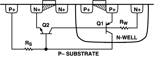
Figure 5. Cross-section of a CMOS inverter with the parasitic structures involved in the thyristor effect.
It is seen that two bipolar transistors form a pnpn-structure (source-pocket-substrate-source), known as a thyristor. VAC of the thyristor is shown in the figure and is characteristic of the fact that it has nonlinearity, that is, when a certain forward bias is achieved on the structure, its resistance drops sharply and the current, respectively, increases.
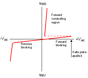
Figure 6. Voltage-ampere characteristic of thyristor.
When an HRT hits, the induced current pulse can lead to the opening of the bipolar transistors and the parasitic thyristor structure to fall into a low-resistance state. The result will be the formation of a short circuit between the ground and power, loss of operability of the affected element and a sharp increase in current consumption, which can lead to "burning out" of the affected element and functional failure. The thyristor effect is referred to as conditionally hard, because its effect can be stopped by resetting the power from the affected chip. This measure, however, is very inconvenient and, with a large number of failures, is inapplicable; The thyristor effect is one of the main headaches of the developers of electronic equipment for space, especially if for some reason they use commercial chips instead of specially designed ones.
How to deal with thyristor effect? You can spread the transistors further from each other, thus increasing the base length of the transistor Q2, but this option is undesirable because of the decrease in the packing density of the crystal.You can increase the levels of doping of the substrate and pocket, reducing the mobility of charge carriers - but this will reduce the speed of the main transistors too.
The most convenient option is to minimize the base impedance of parasitic transistors (Rs and Rw). The smaller the resistance, the less open the emitter pn junction when current flows, and the less likely it is that bipolar charge multiplication is turned on. Technologically, the reduction of basic resistances means ensuring good contacts to the substrate and the pocket, or the creation of transistors in a low-alloyed epitaxial layer grown over a high-alloyed substrate.
The most reliable way to minimize contact resistance to the pocket and the substrate in traditional CMOS technology is by surrounding the transistor with a ring contact (the so-called “guard rings” or guard rings). Depending on the technology and the stringency of the requirements, guard rings can be from one to four (for example, in I / O circuits, where due to the flow of large operating currents, the thyristor effect is also possible for non-radiation-related reasons, including electrostatic breakdown). The obvious drawback of guard rings is a serious increase in the area of the elements (up to several times), that is, even without taking into account other methods of increasing radiation resistance, much fewer transistors will fit on a chip than on a similar non-radiation resistant one.
Another option for protection against the thyristor effect is the complete electrical isolation of each transistor in the circuit, implemented in the silicon-on-insulator technology (SOI), in English, Silicon on Insulator or SOI. A historically important type of SOI is silicon on sapphire (SOS), in which individual silicon islands are grown on the surface of a sapphire monocrystal, but during the transition to small design standards, it was almost completely abandoned for technological reasons, and now under silicon on an insulator is almost always implied silicon on SiO 2 . There are different technologies for creating such plates, but they all boil down to the fact that a relatively thick layer of SiO 2 is formed on the silicon substrate.(called latent or buried oxide or buried oxide), and on top of it is a continuous layer of silicon in which transistors are made, which are separated by conventional side insulation, reaching the hidden oxide. Comparison of cross-sections of MOSFETs made on bulk and SOI technology is shown in Figure NUM. It also shows the pn-transitions, near which the separation of electron-hole pairs.
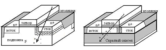
Figure 7. Cross-section of MOSFETs made on bulk and SOI technology. The generation of charge is shown when a heavy charged particle hits.
The complete absence in the SOI of the thyristor effect has led to the fact that even among the specialists who develop the equipment, the “SOI is equal to radiation resistance” is still prevalent, but in reality this is not so. Having an indisputable advantage in resistance to one effect (and that is expressed mainly in saving space on guard rings), SOI can have significantly lower resistance to both the total absorbed dose and to single faults.
The electrical isolation of transistors makes it possible to completely eliminate inter-transistor leaks, but the leakage along the side edges does not disappear and, moreover, the presence of a hidden oxide leads to the appearance of two more transition zones between the oxides - and a parasitic channel can also form on the border of the most hidden oxide. However, the dose stability of SOI schemes is comparable to similar bulk ones, and most of the methods for its improvement in volumetric technology are applicable to SOI.
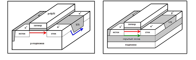
Figure 8. Comparison of the locations of leakage currents in a volume and SOI MOS transistors.
From the point of view of single effects, SOI technology has an important advantage over volume: the area from which diffusion charge collection occurs is limited to latent oxide and is approximately an order of magnitude smaller than in a similar volume technology — that is, the cross section for faults in the saturation region will be an order of magnitude smaller ( and also much shorter than the front of the pulse). Unfortunately, in commercial SOI circuits, this advantage is completely crossed out by the fact that the threshold LET of failure is so low that the intensity of failures is higher for SOI - due to the large number of particles with small LET, which do not knock transistors of volumetric technology, but knock down SOI transistors. The reason for this is the parasitic bipolar effect. You may have noticed from the figures that if the potential of the gate region of the bulk transistors coincides with the potential of the substrate or pocket,then the potential of the gate region of the SOI of the MOS transistor is not controlled by anything. If the TZCH enters the gate area, it can accumulate a charge sufficient to significantly increase the potential. The gate area, bounded above, below and from the sides by the dielectric, and from the remaining two sides by pn junctions, in this situation plays the role of a capacitor charged by the induced heat current. Increasing the potential of the gate region leads to the opening of the source pn junction. Further, a parasitic bipolar transistor is turned on in the MOS transistor, which amplifies the induced THF current pulse by an appropriate number of times (the gain of such parasitic structures can be from a few to about ten). Bipolar multiplication leads to the fact that the critical charge of the element failure decreases several times,and with it, the threshold LET failure, which makes the SOI CMOS circuitry much less fail-safe than similar bulk ones.
Is it possible to get rid of the parasitic bipolar effect? Of course, you only need to make sure that the potential of the gate area is under control. Option two is to make the silicon layer thin enough so that it becomes a channel of the transistor (this is called a fully depleted SOI or full depleted SOI), or create contacts to the gate area. Contacts are of two types: independent and tying the potential of the gate area to the potential of the source.
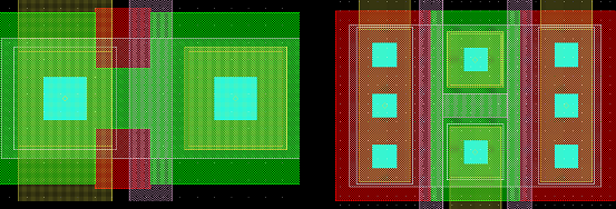
Figure 9. Varieties of contacts to the gate region of a SOI MOS transistor. Green shows n-doping, red - p-doping.
The main advantage of the contact connecting the gate area with the source is compactness, the main drawback is the impossibility of using for some inclusions (for example, in a pass wrench). Independent contacts can be used anywhere, but their area is comparable to the area of the transistor itself, so they are placed only where it is really necessary. In addition, the contacts of both types have another useful property - they overlap the places of formation of parasitic channels and allow, thus, to increase the resistance of the chip to the total absorbed dose.
The techniques shown above make it possible to provide SOI technology with comparable indicators of resistance to the full dose and a smaller by an order of magnitude cross section of saturation of single failures, but the threshold LLE failures are still small enough for the microcircuit that is in orbit to be lost often. It is possible to reduce the frequency of single failures with the help of circuit engineering and systems engineering techniques, but this is a topic for a separate article (or hundreds of dissertations).
Two 1.3 GHz ARMv7 cores
RAM - 1 GB.
Technological process with design standards 150 nm.
Single core PowerPC with a clock frequency of 200 MHz.
RAM - 256 MB.
Above - the parameters of the CPU iPhone5, below - the Curiosity rover. The on-board computer of the rover costs about two hundred times more than the new iPhone. Why is that? The central processor of the spacecraft is exposed to radiation. Habré already had a good overview article on space electronics, and I will try to tell you more about the physical principles and effects behind the failures and failures in space.
Figure 1. The cost of single-board computers RAD company BAE Systems is measured in hundreds of thousands of dollars.
')
The main sources of radiation are the sun and stars. Our own body supplies us with protons and electrons; from the rest of the stars everything flies, including, for example, the nuclei of heavy elements. The inhabitants of the Earth are protected from radiation by a magnetic field that collects particles flying into the radiation belts of the earth (also called van Allen belts). They are also a serious problem for spacecraft, so they try to minimize the time they spend in the radiation belts.
Figure 2. Earth's radiation belts.
What happens when a chip gets into space? There are two main effects - accumulation of the total absorbed dose (total ionizing dose, TID) and effects associated with exposure to single ionizing particles (Single Event Effects, SEE).
The total absorbed dose of radiation causes the drift of some characteristics of the chip, causing failures. The most important mechanisms vary from technology to technology; For modern microcircuits, radiation induced leakage currents are relevant, and in old technologies, the shift of the threshold voltage of the transistor played an important role.
Under the action of ionizing radiation, an electron-hole pair is formed in the microcircuit. Under normal conditions, these pairs quickly recombine (that is, a detached electron is captured by an atom back), but in an electric field, holes and electrons can separate (because the charges of opposite sign move in the field in different directions). The main insulator used in silicon chips is silicon dioxide (SiO 2 ). The mobility of electrons and holes in SiO 2 differs by several orders of magnitude; therefore, electrons are rapidly removed by silicon, and holes can accumulate in the oxide, and especially at the oxide – silicon interface.
If the charge has accumulated in the gate dielectric of the MOSFET, it will affect its operation as an additionally applied positive voltage (or as a threshold voltage shift). As a result, the n-channel transistor will be constantly ajar. In older technologies with thick gate dielectrics, the shift of the threshold voltage of n-channel transistors could be large enough for the transistor to completely stop closing, which naturally led to a loss of circuit performance. However, reducing the threshold voltage even earlier led to the fact that the total current consumption of the chip exceeded the permissible level due to leakage.
In modern technology, the thickness of the gate dielectric is a few nanometers, and they simply cannot accumulate enough holes for the threshold voltage of the transistor to seriously change. Therefore, the determining role is played by charge accumulation in other oxides present in the chip, namely, in the side insulation separating neighboring transistors, and at its boundary in the gate dielectric. The figure shows the cross section of the MOS transistor along the gate. The light layer is silicon, the dark one is SiO 2 . It is clearly seen that the side insulation is much thicker than the gate dielectric. The difference between pictures (a) and (b) is associated with various methods of making insulation and plays an important role in the radiation resistance of the transistor.
Figure 3. Section MOS structures with side insulation type LOCOS and STI.
In a thick insulating dielectric, the electric field is very small, and the separation of electron-hole pairs proceeds poorly. The field dielectric field is large, but the oxide itself is thin. But in the transition region, everything is good (that is, everything is bad) - the oxide is thick enough to accumulate charge in it, and the electric field is large enough that the holes and electrons are effectively separated.
The transistor in the microcircuit can be represented as a superposition of the actual transistor and two lateral parasitic transistors, in which the transition layer between the gate dielectric of the main transistor and the side insulation plays the role of a gate dielectric. The threshold voltage of the main transistor under the influence of the radiation dose varies little, but the threshold of parasitic structures can be reduced to zero, creating current flow channels not controlled by the gate. Through these channels, the current flows freely from the drain to the source — this is called the leakage current.
Leaks, as I said above, lead to an increase in the current consumption of the circuit (which may be unacceptable in a spacecraft, where the available power is very modest) and even to functional failures. For example, the most common problem with flash memory is not associated with storage elements, but with a high voltage generator used for rewriting. There are keys in this generator that, due to leaks, stop closing completely, without which it is impossible to form a voltage sufficient to overwrite the memory.
Single effects occur when a single ionizing particle (proton, neutron or nucleus of a heavier element) enters the transistor and is divided into “soft” (malfunctions) and “hard” (failures). The latter are quite a rare phenomenon characteristic of powerful circuits and poorly understood. Failure options include breakdown of the gate dielectric and burnout of the transistor due to the occurrence of the conducting channel between the drain and the source, as well as the thyristor effect, which I will dwell on in more detail later.
Soft failures have two main mechanisms — primary and secondary ionization. The first is characteristic of heavy charged particles (HTS; in this context they call all nuclei heavier than a proton), the second is for protons and neutrons. Flying through the microcircuit, the particle is inhibited due to the interaction with the crystal lattice and gives it some of its energy (this process can be compared with heating by friction).
The energy released during the passage of a particle ionizes the silicon atoms. Under normal conditions, the overwhelming majority of electrons torn from atoms come back, but if ionization occurs near a strong electric field, it can separate electrons and holes. The mechanism is similar to what happens with dose accumulation, but charge carriers cannot accumulate in silicon, and the duration of single effects is not measured in months, but in picoseconds.
A strong electric field in silicon is the source pn junction of a closed transistor, the separation of a charge near which leads to the fact that charge carriers of one sign fall into the ground / power line, and the second to the drain of the transistor. From the point of view of an external observer, the result of the process looks like a current pulse with a leading edge of several tens of picoseconds and a rear edge of several hundreds. The exact parameters of the pulse depend on many factors, including the technology of making the chip, the angle of incidence of the particle, etc.
If we integrate the resulting current pulse over time, we will get the full charge that is released as a result of the drop in the TZCH. The minimum charge leading to a failure is called the critical charge. The critical charge depends on the parameters of both the affected circuit and the incident particle; In addition, it is very difficult to measure experimentally, so it is usually used to simulate the interaction of a circuit and a particle and for comparative simulation of the failure resistance of different circuits.
Energy release is usually expressed using linear energy transfer (LET; the English term is Linear Energy Transfer, LET), measured in MeV × cm 2 / mg or more precisely, in (MeV / (mg / cm 3 )) / cm. One LET unit is the amount of energy emitted by a flying particle per centimeter of flying distance per unit density of the substance through which the particle flies. The definition at first glance is very confusing, but the unit of measurement chosen in this way has several important advantages: first, the numerical value is relatively easy to measure experimentally; secondly, thirdly, the values used in practice usually fall within the range from one to hundred.
LET - the value is not constant, that is, the parameters of the particle flying at the chip case cover, at the crystal boundary and directly at the transistor, under the numerous layers will be different. From this, however, it does not follow that a thicker body can help - the dependence of LET on the distance traveled in silicon usually has a maximum at a certain depth (the so-called Bragg peak). A similar effect is used in radiation therapy and in some operations for the manufacture of microcircuits: the parameters of implantable ions are chosen so that they stop at a certain depth and create a layer with a high doping level at depth.
Protons and neutrons have very small LET (approximately 0.01 MeV × cm 2 / mg), however, when a high-energy proton / neutron passes through silicon, there is a possibility of a nuclear reaction, the products of which are ions with a short mileage but a large LET (up to 15 MeV × cm 2 / mg). In technological processes with not aluminum, but copper metallization (180 nm and below), moreover, mechanisms of interaction of protons with tungsten, used for contacts of the first level (and located, thus, directly above sensitive pn junctions) are described. LET products of such reactions can reach 30 MeV × cm 2 / mg.
Typical minimum LET of incident particles, resulting in failure - within a dozen for technologies with design standards of 500-250 nm, and about one unit for sub-100 nm technologies, in which the critical charge can be so small that even primary ionization from protons and neutrons can cause a crash. In addition, a small critical charge failure leads to the fact that a sufficient charge can separate when a particle passes not only through the reverse-shifted stock pn-transition, but also through an unbiased source one, which significantly increases the vulnerable area on the crystal.
A short current pulse is perceived by the microcircuit as a pulse noise, and if its amplitude is sufficiently large, it can lead to switching of the element behind the affected transistor - this is a radiation-induced failure. Combination and analog circuits at the time of passage of a current pulse produces an incorrect result, and the storage elements are switched for good. Thus, the most vulnerable part of the microprocessor is the cache memory: there is a lot of it on the chip, and failures in it do not pass by themselves.
Figure 4. Diagram of a six-transistor storage element.
For example, it is most convenient to describe the failure mechanism in a six-transistor static memory cell (the simplest used storage element). The storage element consists of two inverters connected by positive feedback (M1-M2 and M3-M4) and two keys (M5-M6). In the storage mode, two transistors are closed, and two are open, and opposite values are at the inverter outputs. Let for certainty open transistors M1 and M4. When an HRC gets into the drain of a closed transistor (M2 or M3), a pulse of ionization current arises, and two processes start in the cell: positive feedback is triggered and the induced charge is resorbed. These processes are independent (their time constants are determined by different transistors) and competing (the effects of the effects of the processes are opposite).
Let the hit occur in the transistor, the closed transistor M2, on the drain of which a current pulse appeared as a result. The transistor M1 at this moment is fully open and has a small resistance, that is, the induced THC current passes through it into the ground. However, the capacity of the nQ node may be large enough for its potential of this node to grow for a considerable time. An increase in the nQ node potential leads to the switching of the second inverter (M3-M4). In this case, the output voltage of the second inverter varies in such a way that the resistance of the transistor M1 increases, and the transistor M2 opens slightly. If this process takes longer than the charge resorption process, the storage element switches, and the wrong value is recorded in it - this is a radiation-induced failure (single event upset, SEU).
Failures in the combinational logic are somewhat simpler than failures in the storage elements - there is no feedback, and the potential increase of the affected node is directly transmitted to the next cascade. If the voltage amplitude is large enough, the next cascade switches - and then the transition process (single event transient, “needle” in Russian jargon) spreads. Failures in the combinational logic are associated with additional effects that affect how the circuit reacts to the failure. On the one hand, there is a logical masking effect: not all changes in input states affect the output of the circuit (for example, switching one of the inputs of the 2INE element does not affect the output if there is a logical zero at the second input). On the other hand, if the output of the affected circuit is loaded with several elements, then the failure will fall on the inputs of each of them (imagine the failure at the very beginning of the clock signal tree). And finally, time masking: at the output of any combinational circuit, there is a trigger that stores values in certain time intervals. When operating at low frequencies, the probability that the entire pulse will occur during the time at which the trigger does not remember anything is quite large, but with increasing frequency, the pulse duration (from several hundred picoseconds to nanosecond) turns out to be comparable to the period of the clock signal, and for large clocks Frequencies the intensity of significant failures in the combinational logic can be even higher than the intensity of failures in the storage elements (by the way, there can also be failures in the triggers at the outputs of combinational circuits).
The effective track diameter of the SFC is of the order of microns, which is significantly larger than the sizes of the logic elements in modern technologies. Therefore, from hitting a single particle, several elements can get off simultaneously, for example, cache cells. In the technology of 65 nm, “several” can be ten, which creates significant difficulties in the application of noise-resistant codes and forces to seriously modify the topology of the elements of the microcircuit.
When TZCH enters the transistor, there can be not only a single failure, but also a conditionally hard failure caused by the thyristor effect (“latch” or latchup in professional jargon). The figure shows the cross section of the inverter, made by volumetric CMOS technology, and shows the parasitic elements formed by the layers of the chip.
Figure 5. Cross-section of a CMOS inverter with the parasitic structures involved in the thyristor effect.
It is seen that two bipolar transistors form a pnpn-structure (source-pocket-substrate-source), known as a thyristor. VAC of the thyristor is shown in the figure and is characteristic of the fact that it has nonlinearity, that is, when a certain forward bias is achieved on the structure, its resistance drops sharply and the current, respectively, increases.
Figure 6. Voltage-ampere characteristic of thyristor.
When an HRT hits, the induced current pulse can lead to the opening of the bipolar transistors and the parasitic thyristor structure to fall into a low-resistance state. The result will be the formation of a short circuit between the ground and power, loss of operability of the affected element and a sharp increase in current consumption, which can lead to "burning out" of the affected element and functional failure. The thyristor effect is referred to as conditionally hard, because its effect can be stopped by resetting the power from the affected chip. This measure, however, is very inconvenient and, with a large number of failures, is inapplicable; The thyristor effect is one of the main headaches of the developers of electronic equipment for space, especially if for some reason they use commercial chips instead of specially designed ones.
How to deal with thyristor effect? You can spread the transistors further from each other, thus increasing the base length of the transistor Q2, but this option is undesirable because of the decrease in the packing density of the crystal.You can increase the levels of doping of the substrate and pocket, reducing the mobility of charge carriers - but this will reduce the speed of the main transistors too.
The most convenient option is to minimize the base impedance of parasitic transistors (Rs and Rw). The smaller the resistance, the less open the emitter pn junction when current flows, and the less likely it is that bipolar charge multiplication is turned on. Technologically, the reduction of basic resistances means ensuring good contacts to the substrate and the pocket, or the creation of transistors in a low-alloyed epitaxial layer grown over a high-alloyed substrate.
The most reliable way to minimize contact resistance to the pocket and the substrate in traditional CMOS technology is by surrounding the transistor with a ring contact (the so-called “guard rings” or guard rings). Depending on the technology and the stringency of the requirements, guard rings can be from one to four (for example, in I / O circuits, where due to the flow of large operating currents, the thyristor effect is also possible for non-radiation-related reasons, including electrostatic breakdown). The obvious drawback of guard rings is a serious increase in the area of the elements (up to several times), that is, even without taking into account other methods of increasing radiation resistance, much fewer transistors will fit on a chip than on a similar non-radiation resistant one.
Another option for protection against the thyristor effect is the complete electrical isolation of each transistor in the circuit, implemented in the silicon-on-insulator technology (SOI), in English, Silicon on Insulator or SOI. A historically important type of SOI is silicon on sapphire (SOS), in which individual silicon islands are grown on the surface of a sapphire monocrystal, but during the transition to small design standards, it was almost completely abandoned for technological reasons, and now under silicon on an insulator is almost always implied silicon on SiO 2 . There are different technologies for creating such plates, but they all boil down to the fact that a relatively thick layer of SiO 2 is formed on the silicon substrate.(called latent or buried oxide or buried oxide), and on top of it is a continuous layer of silicon in which transistors are made, which are separated by conventional side insulation, reaching the hidden oxide. Comparison of cross-sections of MOSFETs made on bulk and SOI technology is shown in Figure NUM. It also shows the pn-transitions, near which the separation of electron-hole pairs.
Figure 7. Cross-section of MOSFETs made on bulk and SOI technology. The generation of charge is shown when a heavy charged particle hits.
The complete absence in the SOI of the thyristor effect has led to the fact that even among the specialists who develop the equipment, the “SOI is equal to radiation resistance” is still prevalent, but in reality this is not so. Having an indisputable advantage in resistance to one effect (and that is expressed mainly in saving space on guard rings), SOI can have significantly lower resistance to both the total absorbed dose and to single faults.
The electrical isolation of transistors makes it possible to completely eliminate inter-transistor leaks, but the leakage along the side edges does not disappear and, moreover, the presence of a hidden oxide leads to the appearance of two more transition zones between the oxides - and a parasitic channel can also form on the border of the most hidden oxide. However, the dose stability of SOI schemes is comparable to similar bulk ones, and most of the methods for its improvement in volumetric technology are applicable to SOI.
Figure 8. Comparison of the locations of leakage currents in a volume and SOI MOS transistors.
From the point of view of single effects, SOI technology has an important advantage over volume: the area from which diffusion charge collection occurs is limited to latent oxide and is approximately an order of magnitude smaller than in a similar volume technology — that is, the cross section for faults in the saturation region will be an order of magnitude smaller ( and also much shorter than the front of the pulse). Unfortunately, in commercial SOI circuits, this advantage is completely crossed out by the fact that the threshold LET of failure is so low that the intensity of failures is higher for SOI - due to the large number of particles with small LET, which do not knock transistors of volumetric technology, but knock down SOI transistors. The reason for this is the parasitic bipolar effect. You may have noticed from the figures that if the potential of the gate region of the bulk transistors coincides with the potential of the substrate or pocket,then the potential of the gate region of the SOI of the MOS transistor is not controlled by anything. If the TZCH enters the gate area, it can accumulate a charge sufficient to significantly increase the potential. The gate area, bounded above, below and from the sides by the dielectric, and from the remaining two sides by pn junctions, in this situation plays the role of a capacitor charged by the induced heat current. Increasing the potential of the gate region leads to the opening of the source pn junction. Further, a parasitic bipolar transistor is turned on in the MOS transistor, which amplifies the induced THF current pulse by an appropriate number of times (the gain of such parasitic structures can be from a few to about ten). Bipolar multiplication leads to the fact that the critical charge of the element failure decreases several times,and with it, the threshold LET failure, which makes the SOI CMOS circuitry much less fail-safe than similar bulk ones.
Is it possible to get rid of the parasitic bipolar effect? Of course, you only need to make sure that the potential of the gate area is under control. Option two is to make the silicon layer thin enough so that it becomes a channel of the transistor (this is called a fully depleted SOI or full depleted SOI), or create contacts to the gate area. Contacts are of two types: independent and tying the potential of the gate area to the potential of the source.
Figure 9. Varieties of contacts to the gate region of a SOI MOS transistor. Green shows n-doping, red - p-doping.
The main advantage of the contact connecting the gate area with the source is compactness, the main drawback is the impossibility of using for some inclusions (for example, in a pass wrench). Independent contacts can be used anywhere, but their area is comparable to the area of the transistor itself, so they are placed only where it is really necessary. In addition, the contacts of both types have another useful property - they overlap the places of formation of parasitic channels and allow, thus, to increase the resistance of the chip to the total absorbed dose.
The techniques shown above make it possible to provide SOI technology with comparable indicators of resistance to the full dose and a smaller by an order of magnitude cross section of saturation of single failures, but the threshold LLE failures are still small enough for the microcircuit that is in orbit to be lost often. It is possible to reduce the frequency of single failures with the help of circuit engineering and systems engineering techniques, but this is a topic for a separate article (or hundreds of dissertations).
Source: https://habr.com/ru/post/189066/
All Articles