Making microcircuits at home - part 3
 A little more than a year has passed since the previous articles about my project of creating microcircuits at home ( 1 , 2 ), people continue to be interested in the results - which means it's time to talk about progress.
Let me remind you of the project’s goal: to learn how to make simple silicon digital chips in “home” conditions. This will in no way allow to compete with mass production - besides the fact that it is orders of magnitude more advanced (~ 22nm against ~ 20µm, each transistor is a million times smaller in area), it is also monstrously cheap (this item did not immediately become obvious). Nevertheless, even the simplest working chips made at home will have at least an educational and of course decorative value.
Let's start with setbacks and drama
As I already mentioned in the comments to another topic, an attempt to get kickstarter with this project failed - the project did not pass moderation due to the lack of a prototype. This forced once again to rethink the ways of commercialization of this simplified technology. The possibility of releasing a home chip technology in the form of a RepRap-like opensource whale is covered in fog: there is too much dangerous, expensive and unstable chemistry - it will not be so easy to send by mail. It also seems that there is no possibility to make smaller lots of microcircuits cheaper than serial plants: now the minimum test batches of microcircuits can be made about $ 30-50 each (in a batch of ~ 25 pieces), and it is much cheaper than $ 30 per chip to make it on a self-made simplified installation . In addition, despite the low price in conventional factories - practically no one does amateur chips, there are practically no tasks where they would have advantages over FPGA / CPLD / microcontrollers, and the cost and complexity of development remains very high.')
But as I mentioned above, even with these shortcomings, the project remains interesting for me.
Logistics
From what has already been mentioned in my other articles in recent months - an oxygen concentrator has been purchased, which makes it possible to get ~ 95% oxygen without a headache. Of the harmful impurities - it looks like only carbon dioxide (35ppm), let's hope this will be enough. There is also an ozone generator coming from China (it needs oxygen at the entrance) - there are research results showing that it is convenient for them to grow thin gate dielectrics and use them as one of the steps to clean the plates.
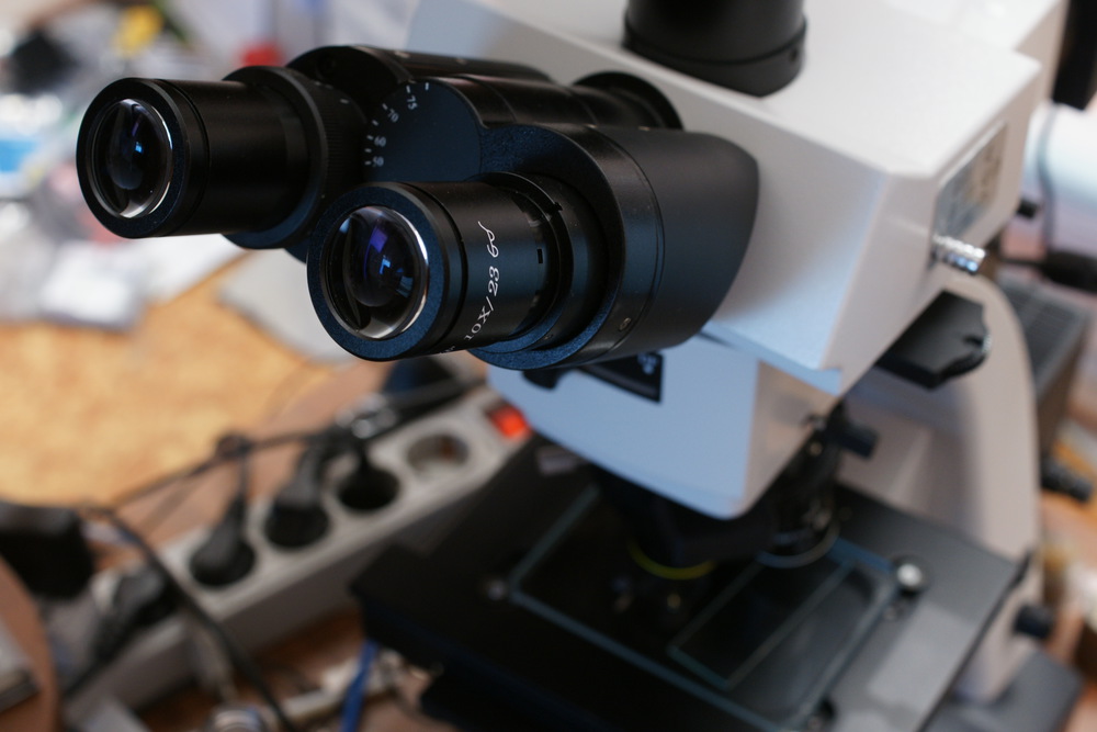
A metallographic microscope has been bought for a long time, and heaps of existing microcircuits have been investigated . In general, it has become much clearer to deal with. Finally, since a microscope is a symmetrical device, it can be used to project a reduced image in photolithography. The combination of images - visual and manual. The source of illumination for projection is not even necessary to do a UV diode, white light is also quite suitable - the image quality allows (although I also have powerful 405nm diodes). The photolithographic standards achieved in this way are micron-based (if you try hard, then up to ~ 350 nm), but there is no point in greatly reducing transistors, since “frame size” is also reduced proportionally, contacts to which will have to be welded out will become too small. So, initially we will have to limit ourselves to the norms of 10-20 mkm, as planned.
The microscope somewhat shaken the faith in both domestic producers and in Chinese. It turned out that some of the “domestic” microscopes are remarked Chinese for 200-300% of the price. On the other hand, one of the lenses seems a bit crooked and the stage table had a slight casting defect - I had to modify it with a file (in the literal sense of the word).
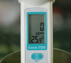
One of the important chemical elements for the production of microchips is water. Again, in China, a conductivity meter was purchased - a measure of the electrical conductivity of water. The conductivity can be used to estimate the amount of dissolved salts (+ -50%, if it is not known what exactly is dissolved). Salts of potassium, sodium, calcium, and manganese are usually dissolved in water — all of which are very dangerous for microchips (especially sodium and potassium), since their ions can move rapidly in silicon and silicon oxide at ordinary temperatures and change the electrical parameters of transistors (for field-effect transistors, threshold voltage, leakage).
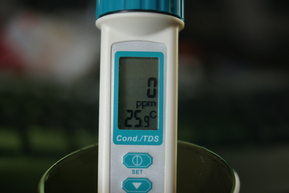
Measured the available water samples, and received the following:
| Impurity concentration | |
| Tap water | 219ppm |
| "New" household filter | 118ppm |
| "Old" household filter | 210ppm |
| Boiled water from the new filter | 140ppm (!!! 2 times rechecked) |
| Redistilled water from Ruskhim (Unlike double distilled) | 10ppm |
| Deionized water from the Institute of Microbiology | 0ppm |
| Deionized after 6 hours in the air (Due to dissolution of carbon dioxide from the air) | 8ppm |


Also managed to buy and TMAH (tetramethylammonium hydroxide) - used as a developer for photoresist, not containing alkali metal ions (which as we know - evil).

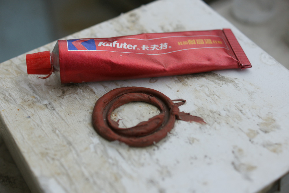
For a vacuum system - instead of buying vacuum rubber (I tried several times - but never mastered it), there was such a gasket maker in China - a paste that can be squeezed into the desired shape, it hardens - and becomes rubber.
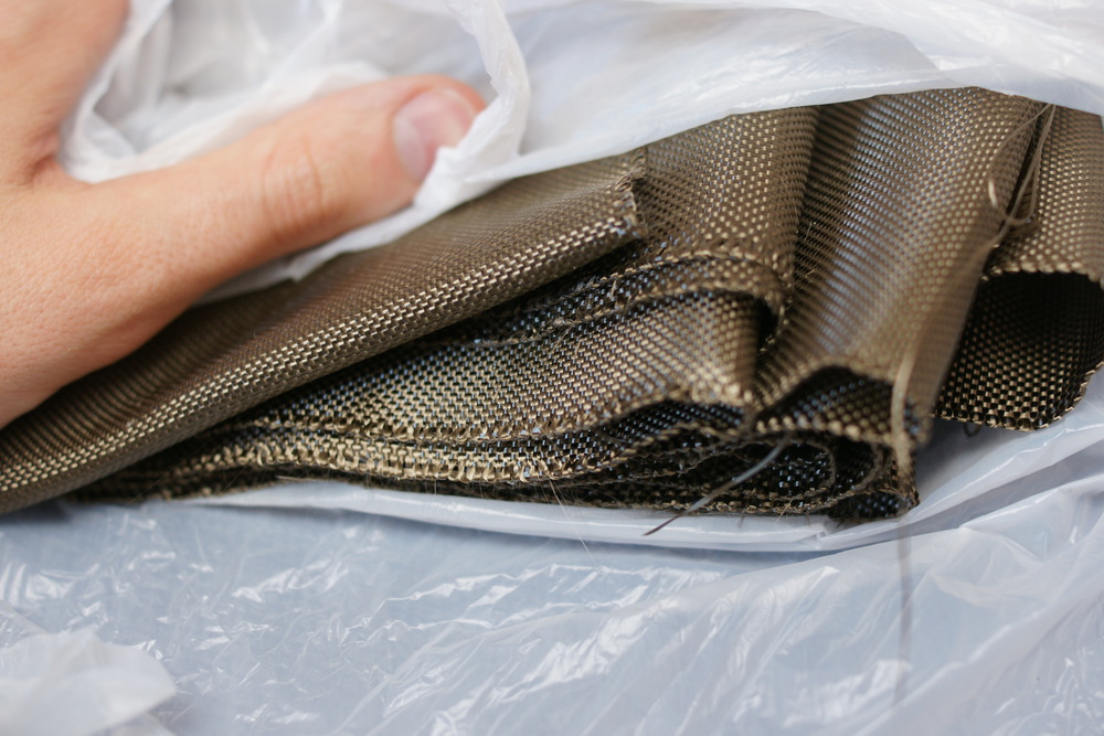
On the stove: for thermal insulation - such basalt cloth was bought, it is used for thermal insulation of nuclear reactors. Maintains 1000-1200 degrees.
Under the microscope - you can see the individual strands of molten basalt, of which the canvas is woven. These are real nanotechnologies !!! In the head at first does not fit: how can you make a stone of the thinnest thread, and weave a flexible material? (scale: 1 pixel ~ 3 micrometers):

Quartz tubes for stoves of different diameters found and cut. The first level of thermal insulation is the air gap between the tubes inserted into each other.

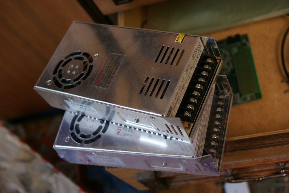
Initially, I thought of feeding the stove directly from 220 volts - but still, it was prudent to switch to 48 volt DC power — this would allow both control and control of power to be more accurate, and make the design safer. Bought 2 power supply 400W. How the Chinese make such a unit and deliver for $ 19 is a mystery:
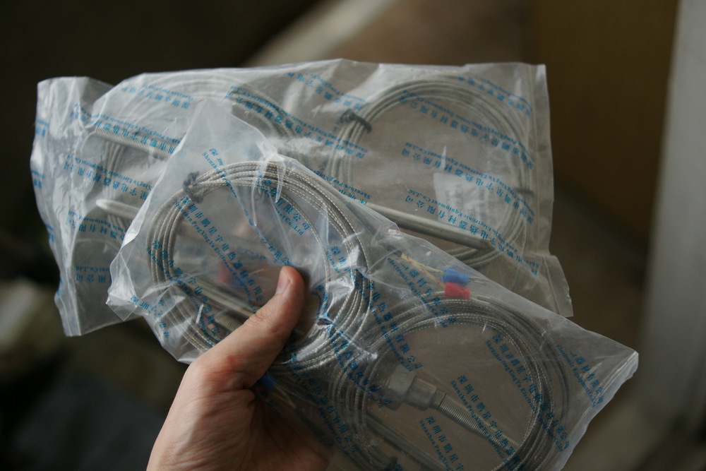
To control the temperature, high-temperature thermocouples designed for 1200 degrees were originally purchased (I wrote about them in the last series, but there was no photo). The size of course horse. It will probably be easier to monitor the level of infrared radiation at a wavelength of 1 micron - quartz is transparent to it.
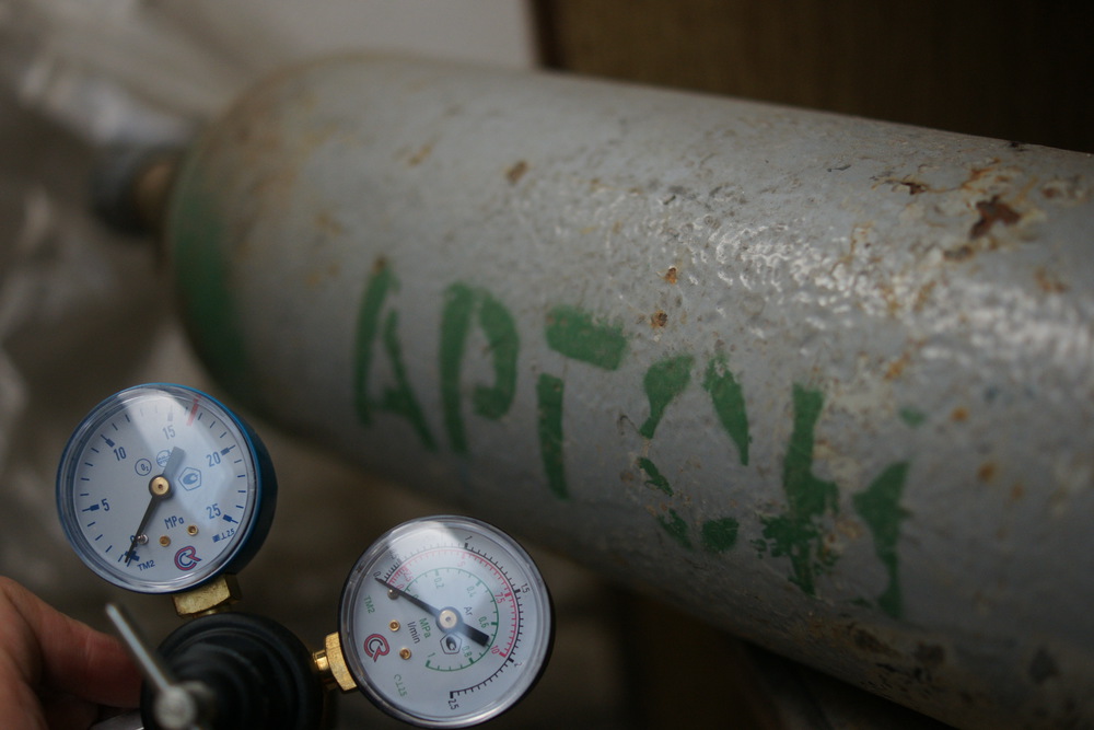
And finally - an inert environment for the stove. In my case, this is Argon. Due to the nature of the separation of gases, argon is cleaner than nitrogen, although it is somewhat more expensive. I bought a small 10l bottle and regulator. The regulator did not suddenly fit - the thread does not match, you need to either look for an adapter, or buy another regulator.
It turned out that compressed gases are sold near the house (life in the industrial zone of Moscow has its advantages) - and I came for it with a trolley. The worker did not appreciate my impulse - and strongly recommended wrapping the container in cardboard so that passersby would not worry. In 15 minutes we coped with camouflage. In general, a meeting with the real world always gives surprises :-)
Software and development
The most important thing is that we managed to thoroughly understand how microcircuits work with NMOS technology, why there are 3 supply voltages (or 2, with a decrease in speed). Finally, a high-quality open-source software was found for the development of simple microcircuits, including the supporting and NMOS process - gnuelectric :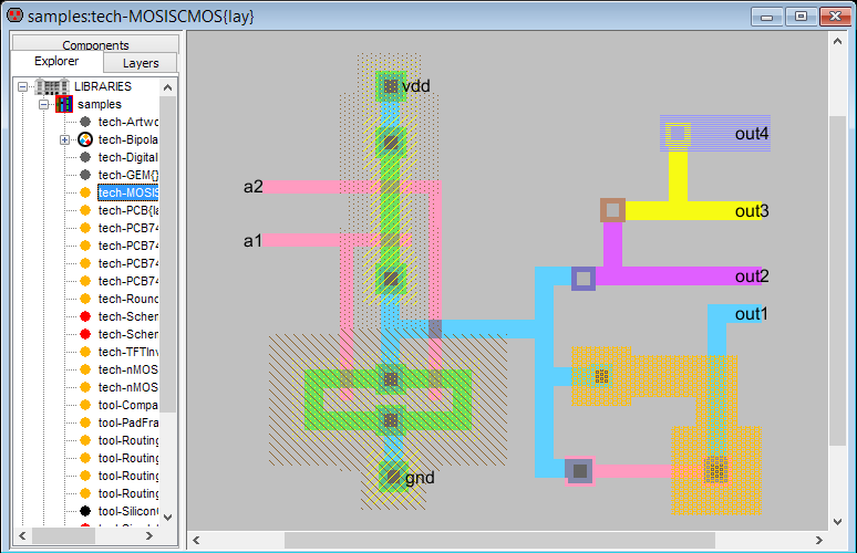
What else is missing
From what I mentioned in the previous article - TEOS is apparently not needed, it is too difficult to work with it, HMDS is not necessary, at least for "large" transistors.The nitrogen generator is of course convenient, working with plates in an inert atmosphere and not messing with cylinders, but also not critical.
The only thing that could seriously facilitate the work is the samples of spin-on dopants and spin-on glass. In Russia, for various reasons, they are not used and not produced; abroad, there are few producers, they are sold in large quantities and are expensive (thousands of dollars). The company Emulsitone, from which it bought Jeri Ellsworth samples when it made its transistors, seemed to be bent, and it was not possible to contact them. But this is also not a mandatory item - you can work without them (with phosphoric and boric acids, POCl3 and BBr3), although it is much more difficult / somewhat more dangerous.
And finally - of course, there is not enough sponsor for my projects, sometimes you have to choose the first one between the extra time and extra money. If someone from companies or individuals has a desire to sponsor my projects (conditions are discussed) - you know where to find me :-).
Update: There is a rough estimate, I send it on request - i.e. There is an idea for what exactly money is needed.
On the "serial" project
In the last article I mentioned my classic microelectronic project - I wanted to develop and produce microcontrollers at production plants. Having researched competitors under a microscope (production standards, area), and having learned the prices of production at almost all plants (both domestic and foreign), it became clear that this business is good, though very capital-intensive. Nonetheless, it does not seem like fate here - the project was turned twice in Skolkovo , due to my lack of specialized experience. On the one hand, they are certainly right, on the other - Zuckerberg would come to Skolkovo, and to him, “And how many social networks have you created?”. Enter into the team of bogus members - absolutely no desire. So, as always, life makes adjustments to rosy plans - you will probably first have to earn money for the project in other ways, and come back to it in 3-5 years time (if someone else needs it then).Future plans
The next step is the assembly of the stove with control electronics, and finally the production of the first samples. For a start, silicon diodes, a study of their characteristics, solar batteries, then field-effect transistors, possibly bipolar. You can try to make Schottky diodes - but things are not so simple with them (high demands on the metal-semiconductor interface and the edges of the diode).Then you need to think about how to make ultrasonic or thermocompression welding of the wire with a silicon wafer at home - this is necessary for connecting the leads.
I hope in the foreseeable future, we all see the home chips :-)
Source: https://habr.com/ru/post/188992/
All Articles