We study STM32 in practice. Part 1. Screen connection from Siemens C55

Disclaimer! The authors do not guarantee the ultimate truth, in any case due to the inexperience in the new sphere. If you see a gross technical error, we kindly ask you to report it as soon as possible!
Brought together somehow the fate of a novice programmer and novice electronics engineer together. And they began to create. They made a dozen small bear toys with recording sound modules and realized that using single-function cards was not so fun. And in the bright summer evenings they gathered and thought, what would make them so interesting? Fate helped them a second time: they found an advertisement for the sale of the STM32VLDiscovery debugging board in Russia and a week later with shaking hands they unpacked the package and "blinked" the LEDs. From the feeling of complete power over a tiny device, my eyes lit up and earned brains. It was decided: to make an “electronic bracelet” with some interesting functionality, using the full potential of their new “toy” ...
The eyes lit up even more when we learned about the possible ways to use the STM32. First of all, we thought about connecting all kinds of peripherals. We had a seven-segment LCD on the hands of the Soviet watches. They hooked up, wrote a timer, but could not calm down ...
')
The next day, we went to a small shop at a service center and were stunned by the huge number of phones for analysis: 3 stands completely filled with various “hits” among the cell phones of previous years. A total of 80 rubles was bought by Siemens C55, which later became our donor.
Having scratched through the case, we got IT: a monochrome LCD screen LPH7999-4 with a resolution of 102 by 64 pixels. It consists of, in fact, the LCD matrix and the PCF8812 controller (link to the datasheet) . The controller also consists of DDRAM, in which pixel states (1 \ 0), I \ O-buffer, several current generators and logic elements are stored in the form of a table, bit by bit. All actions with LCD occur directly with the controller through 8 legs VDD, SCK, MISO, DC, SS, GND, VOUT, RES, of which two are closed through the capacitor, and the rest are connected to the legs of our processor.
At the same time, the thought passed through our heads: “What kind of incomprehensible designations are these and how can we manage this at all?” With an expression of complete sadness and hopelessness, we began to google, constantly bumping into articles full of unknown terms. As a result, after several days, new information has been added to our heads.


| MOSI (or SIMO, SDO, DO, DOUT, SO, MTSR) Master Output Slave Input | Master output, which must be connected to the Slave inputs |
| MISO (or SOMI, SDI, DI, DIN, SI, MRST) Master Input Slave Output | Master's input to which Slave's outputs go |
| SCK (or SCLK, CLK) | supplied clock frequency for "parsing" of bits from MISO \ MOSI |
| SS (or CS) | selection of the peripheral device with which we will work. If there are more than one device, then to work with a specific one, you need to turn OFF the jumper foot on the selected one and ON on all other devices. |
So, to control our LCD, we need to use SPI, a standardized interface for communicating with peripherals. To use it, you need to understand the principle of work and all the terminology associated with it, and in particular the names and purposes of all the legs.
The SPI interface assumes that we have some ONE device that will control everything (Master) and a lot of controlled peripherals, such as sensors, LCD \ LCD, memory cards, ADC \ DAC, etc. (Slave). On our Master, we have to choose 3 legs for receiving / transmitting data and n legs-jumpers, where n is the number of connected peripheral devices. On Slave devices, legs for receiving / sending are usually defined in advance (if this is, of course, not another processor) and are described in the corresponding datasheets.
Let us consider an example of the work of transmitting and receiving data between an abstract Master and one abstract Slave device.
Note! SPI is organized as follows: when transferring data from MOSI Master to MISO Slave, data is transferred simultaneously from MOSI Slave to MISO Master and vice versa. Thus, the SCK signal is the same for MISO and MOSI, respectively, they work the same way.
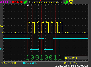
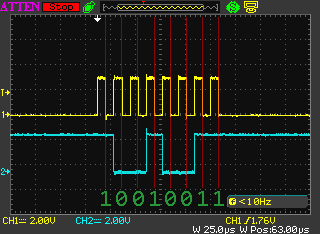
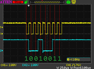
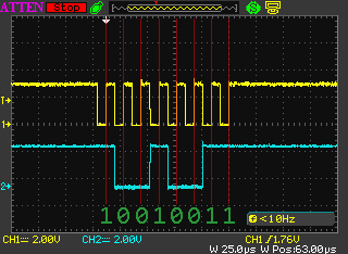
When transmitting one byte, the SCK and MOSI outputs are involved. Our SCK output is clocked pulses (voltage drops from a logical zero to a logical one). When transmitting a logical unit at the output voltage ~ 3.3V, when transmitting zero, respectively ~ 0V. The duration of the state of logical zero and logical unit are equal and are set programmatically. When transmitting one byte, each bit has a pulse. Thus, at the SCK output, when transmitting a byte, we can see eight identical “humps”. At the MOSI output, our information is transmitted directly. For example, if we transmit 10000001, the signal will look like a big pit, and if 10011001, then a pit with a protrusion in the middle. I think it’s clear how both outputs work separately now, but now we’ll tell you how they are coordinated with each other.
In idle mode. The moment when nothing is transmitted, that is, in the interval between the transfer of bytes or before they begin to transmit when SPI is enabled. It would be logical to assume that in the absence of any operations on both inputs would be 0. But no, in the idle mode on MOSI, the voltage of a logical unit, on SCK, is either a logical unit or zero. This is the state of SCK we can choose for ourselves.
In transfer mode. Here we have to choose how the impulses of the SCK and MOSI ports will be matched. To do this, you have to enter a few bad words:
A front is a transition from one state to another, that is, a voltage jump from a logical one to a logical zero. In the image of the pulse, these are vertical sticks.
The front is growing and falling: growing - the transition from a logical zero to a logical one, a falling one - on the contrary, from a logical one to a logical zero.
The front is also the front and rear: the front is the first jump that occurred after the idle mode, the rear edge is the second jump that occurred after the idle mode.
The developer can choose for SCK the idle mode (logical one or zero) and the transfer mode (on the leading or trailing edge). Total, there are 4 modes of operation:
Mode 0 (00):
The idle mode is a logical zero.
Transfer to the leading edge.
Since we chose transmission on the leading edge, during the transition from the voltage of the logical zero to the voltage of the logical unit on the SCK, a bit will be transmitted to the MOSI.
Mode 1 (01):
The idle mode is a logical zero.
Transfer on the falling edge.
Since we chose the transmission on the falling edge, then the rising front comes first, then the voltage of a logical zero lasts for a while, then the falling falling front goes. After that, a bit will be transmitted to MOSI.
Mode 2 (10):
Idle mode is a logical unit.
Transfer to the leading edge.
During transmission, an impulse is sent to SCK. But it is not growing, as opposed to the two previous modes, but falling. Since the voltage of the logical unit of voltage cannot be higher, the first impulse goes "down." It was during this transition (after all, we chose the leading edge) that the bit is transmitted to MOSI.
Mode 3 (11):
Idle mode is a logical unit.
Transfer on the falling edge.
During transmission, the impulse goes to SCK, first falling down, then increasing. At this time there is a transition to MOSI.
Usually, the mode of operation is not indicated in datasheets, but it is easy to get if you study the behavior of MOSI \ MISO and SCK on any chart in the datasheet.

So what can we manage on our controller?
First, we have the memory that the controller displays on the LCD matrix.
Secondly, we have a memory carriage with coordinates X and Y
Third, we have about a dozen different bits:
  Bit PD - if 0, then the controller is on, if 1 - then the controller is in sleep mode
	 Bit V - if 0, then after the data is written, the carriage shifts by X by one, otherwise Y shift by 9 (that is, immediately after the recorded bar)
	 Bit H - if 0, then the mode is enabled to work with the usual set of instructions, if 1 - then with extended
	 Bits D and E are responsible for the display mode:
		 00 - all pixels are off
		 01 - all pixels are lit
		 10 - if the state of a pixel in memory is 1, then it is on, if it is 0, then it is off (normal mode)
		 11 - if the state of a pixel in memory is 1, then it is NOT lit, if 0, then it is lit (inversion)
	 Bits TC1 and TC0 are responsible for the LCD temperature coefficient.
		 00 - coefficient 0
		 01 - coefficient 1
		 10 - coefficient 2
		 11 - coefficient 3
	 Bits S1 and S0 are responsible for the internal power multiplier, i.e.  theoretically how many times the food,
		 filed on VDD will be different from internal power
		 00 - twice as much
		 01 - three times more
		 10 - four times more
		 11 - five times bot
	 Bits Vop6-Vop0 responsible for the magnitude of the original internal voltage
	 The BS2-BS0 bits are responsible for the system offset.
Now we give the possible commands for management. Each of them is formed of exactly 8 bits:
| (in any mode of instructions) | ||||||||
| set registers PD, V, H | 0 | 0 | one | 0 | 0 | PD | V | H |
| (in the usual set of instructions) | ||||||||
| set registers D, E | 0 | 0 | 0 | 0 | one | D | 0 | E |
set the X coordinate of the carriage (  ) ) | one | X 6 | X 5 | X 4 | X 3 | X 2 | X 1 | X 0 |
set the Y coordinate of the carriage (  ) ) | 0 | one | 0 | 0 | Y 3 | Y 2 | Y 1 | Y 0 |
| (in extended instruction set) | ||||||||
| set TC register | 0 | 0 | 0 | 0 | 0 | one | TC 1 | TC 0 |
| set register S | 0 | 0 | 0 | 0 | one | 0 | S 1 | S 0 |
| set BS register | 0 | 0 | 0 | one | 0 | BS 2 | BS 1 | BS 0 |
set register V (  ) ) | 1 V op 5 | V op 6 | V op 5 | V op 4 | V op 3 | V op 2 | V op 1 | V op 0 |
In order to correctly initialize the LCD, we must energize the VDD, disconnect it to the RES, wait 100 µs and apply it to the RES again. When the power to the RES is turned off, the controller goes into sleep mode, the RAM is not guaranteed to be cleared, many of the registers get their default value. You can read more on page 14 in the datasheet on the controller .
After that, we need to turn off the SS (ie, “choose” the device for operation) and turn off the DC (ie, start sending commands) and send several initializing commands using SPI:
- turn on the power, and at the same time set V = 0 and H = 1
- select temperature coefficient TC = 11
- set the maximum internally powered V op = 1111111
- enable internal power factor S = 01
- set the system offset BS = 011
- enable normal instruction set mode H = 0, V = 0, PD = 0
- select the normal display mode D = 1, E = 0
After that, our display will light up and show us random pixels taken from non-RAM.
Unfortunately, there is no MOSI on the controller (i.e. there is no feedback), so if the display does not show anything, then to make sure if at least SPI is working, after the above commands you need to measure the voltage on the 7th leg of the LCD.
Experienced (and long) by clarified the following: if the display does not show anything, but there is voltage on the 7th leg, this means that the SPI works and that the display does not have enough internal voltage and needs to be increased using the V op and S registers , eg). In our case, the display lights up at ~ 6V.

We studied the theory and now proceed to the implementation. There are two ways to implement work with SPI: make everything handles with the help of controlling the legs of the processor (software spi) or use the hardware implementation (hardware spi), which is in our STM32. For example, I see no reason to implement an interface using processor power, so I use hardware spi.
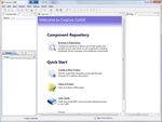
The code will be written and debugged in CooCox IDE:
- Launch CoIDE and create a new project.
- Choose the GPIO modules we need (for controlling the legs), SPI (for controlling SPI), RCC
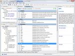
- Let's write a small frame for our future program.
#include "stm32f10x_gpio.h" #include "stm32f10x_rcc.h" #include "stm32f10x_spi.h" void SPIInit(void) { } void GPIOInit(void) { } void LCDInit(void) { } int main() { SystemInit(); GPIOInit(); SPIInit(); LCDInit(); return 0; } - Let's start with filling GPIO. To do this, using the datasheet on the STM32, we must find out where the legs of the “iron” SPI are. Our model is PA5 (SCK), PA6 (MISO), PA7 (MOSI). These legs can be either regular legs or SPI legs, so we need to explicitly state the intended purpose and use them.
- Consider the remaining legs:
Vdd leg to connect power, connects to an arbitrary leg on the STM32 (in our case, on the LPH7999-4, the connection limit is up to 6.5V, and the STM32 produces 3.3V for each of its legs) VOUT output internal power, is connected to the earth screen through the capacitor x mF. GND land see VOUT Res leg to control controller reset, connects to arbitrary leg on STM32 DC the leg responsible for the mode of data transfer to the controller is connected to an arbitrary leg on the STM32. If there is no voltage on the leg, the LCD controller interprets the received data as a command, and if it is, it is interpreted as a set of 8 pixels that will be written as a column in DDRAM relative to the location of the carriage. SS see above, connects to an arbitrary leg on STM32 - We solder SCK, MOSI to PA5 and PA7, and DC, VDD, RES and SS to arbitrary legs. We have PB0, PB1, PB2, PB3, respectively.
- Write the code:
#define SCK_Pin GPIO_Pin_5 #define SCK_Pin_Port GPIOA #define MOSI_Pin GPIO_Pin_7 #define MOSI_Pin_Port GPIOA #define DC_Pin GPIO_Pin_0 #define DC_Pin_Port GPIOB #define VDD_Pin GPIO_Pin_1 #define VDD_Pin_Port GPIOB #define RST_Pin GPIO_Pin_2 #define RST_Pin_Port GPIOB #define SS_Pin GPIO_Pin_3 #define SS_Pin_Port GPIOB void GPIOInit(void) { // (=) A, B SPI1 RCC_APB2PeriphClockCmd(RCC_APB2Periph_GPIOA | RCC_APB2Periph_GPIOB | RCC_APB2Periph_SPI1, ENABLE); GPIO_InitTypeDef PORT; // PORT.GPIO_Pin = SCK_Pin | MOSI_Pin; // ( 4 ) PORT.GPIO_Speed = GPIO_Speed_2MHz; // (!) . - " " PORT.GPIO_Mode = GPIO_Mode_AF_PP; // GPIO_Init(GPIOA, &PORT); // PORT.GPIO_Pin = DC_Pin | VDD_Pin | RST_Pin | SS_Pin; // ( - ) PORT.GPIO_Speed = GPIO_Speed_2MHz; // - , PORT.GPIO_Mode = GPIO_Mode_Out_PP; // B GPIO_Init(GPIOB, &PORT); }
Let's write auxiliary procedures for code readability: void PowerOn() { VDD_Pin_Port->ODR |= VDD_Pin; } void PowerOff() { VDD_Pin_Port->ODR &= ~VDD_Pin; } void ResetOn() { RST_Pin_Port->ODR |= RST_Pin; } void ResetOff() { RST_Pin_Port->ODR &= ~RST_Pin; } void DCOn() { DC_Pin_Port->ODR |= DC_Pin; } void DCOff() { DC_Pin_Port->ODR &= ~DC_Pin; } void SSOff() { SS_Pin_Port->ODR &= ~SS_Pin; } void SSOn() { SS_Pin_Port->ODR |= SS_Pin; }- Now configure SPI:
void SPIInit(void) { SPI_InitTypeDef SPIConf; // , SPIConf.SPI_Direction = SPI_Direction_1Line_Tx; // , - Master SPIConf.SPI_Mode = SPI_Mode_Master; // 8 (=1 ) SPIConf.SPI_DataSize = SPI_DataSize_8b; // 00 SPIConf.SPI_CPOL = SPI_CPOL_Low; SPIConf.SPI_CPHA = SPI_CPHA_1Edge; SPIConf.SPI_NSS = SPI_NSS_Soft; // ( , ) SPIConf.SPI_BaudRatePrescaler = SPI_BaudRatePrescaler_2; // (.. ) SPIConf.SPI_FirstBit = SPI_FirstBit_MSB; // SPI SPI_Init(SPI1, &SPIConf); // SPI1 SPI_Cmd(SPI1, ENABLE); // SS = 1 SPI_NSSInternalSoftwareConfig(SPI1, SPI_NSSInternalSoft_Set); } - Write the function to send data via SPI
void SPISend(uint16_t data) { SPI_I2S_SendData(SPI1, data); // while (SPI_I2S_GetFlagStatus(SPI1, SPI_I2S_FLAG_TXE) == RESET); // , } - Let's add initialization according to theory
void LCDInit(void) { SSOff(); DCOff(); PowerOn(); ResetOff(); ResetOn(); SPISend(0x21); // , , . . SPISend(0b1001); // SPISend(0xFF); // SPISend(0x06); // SPISend(0x13); // bias ( ) SPISend(0x20); // ..., SPISend(0b1100); // } - Project - Build (or F7)
- Flash - Program Download
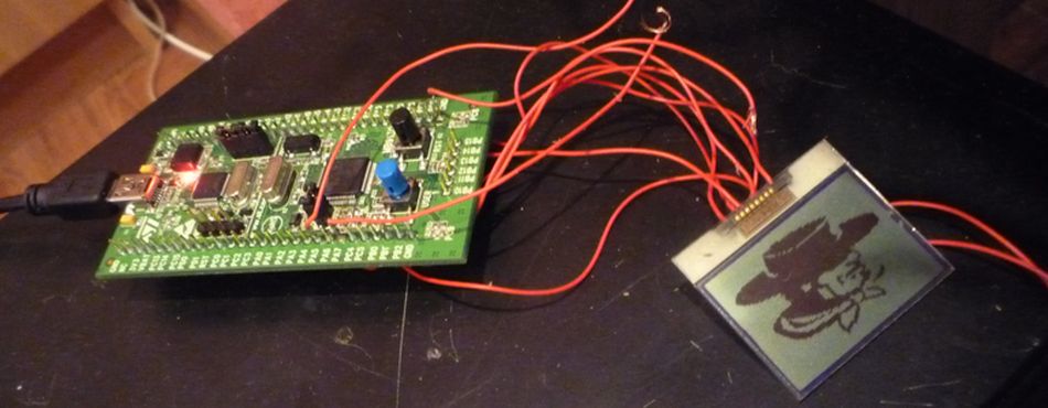
- We look and rejoice: 3
Here you can download the finished project for CooCox.

Of course, to surprise in 2013 with the connected display to the ARM processor is difficult. For us, as for beginner developers, this is the first step towards the realization of our project of a unique “electronic bracelet”.
We do not dream of entering the market, we just want to gain experience, make a functional, stylish and long-lasting gadget for ourselves, and at the same time tell about our successes and failures here.
Now our device is able to draw pictures on the screen, previously converted into an array of 8-bit "columns" using this Python script , requiring Python 2.7 and PIL .
Usage: photo.py file24bit.bmp> bytes.c
Some illustrations were taken from http://easystm32.ru/interfaces/43-spi-interface-part-1
Source: https://habr.com/ru/post/188082/
All Articles