STM32F4Discovery - we connect the camera via DCMI interface
STM32F4Discovery - we connect the camera via DCMI interface
 Once, when connecting a camera from a mobile phone to an STM32F407VGT6 microcontroller (which takes place on the STM32F4Discovery board), I did not even think that this controller has a special hardware interface for this case. Maybe I didn’t read the datasheet inattentively, but I always thought that only the chips in the UFBGA176 and LQFP packages with 144 legs have a DCMI interface. However, not so long ago, I discovered the voiced detail: the 100-legged STM32F407 also has DCMI on board.
Being a great lover of studying and jointly launching various mobile iron (in particular, LCD and cameras) with the MK, I simply could not get past such a discovery, and decided to fill this gap in studying the STM32 periphery. Actually, this material is devoted to the description of the implementation of the arisen venture.
Just a little theory.
')
First of all, you need to imagine what is at stake - or rather, what a CMOS-camera is, and with what it is eaten.
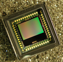
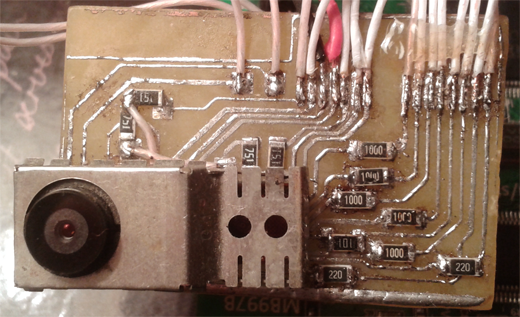
This type of camera provides information output from the sensor in digital form: RGB, YCbCr, and also in compressed form - JPEG. Different cameras have their own nuances in terms of capabilities, I will consider a very specific case of a camera with a small resolution (VGA, 640x480), which I had pulled out from time immemorial from the Siemens C72 phone ( PixelPlus PO2030N sensor). This camera is the most suitable for studying in view of the simplicity of functioning and the type belonging to a more or less common one. A long time ago, I eliminated a small board for it (for greater convenience of connection) - with a 2.8 V stabilizer and pull-up resistors on the I2C bus. Here it is (cable and camera connector hidden under the casing).
In addition to nuances in the field of data format, cameras may also differ in the number of synchronization pins. Most (in my opinion) sensors have special conclusions on line and frame synchronization; but there are cameras that have only a pixel strobe output, and they let know about the beginning of a new line / frame with the help of special transmitted codes (for example, 0x00 or 0xFF ). The camera that I have available has external synchronization pins.
You can estimate the approximate schematic image of the camera as a block.
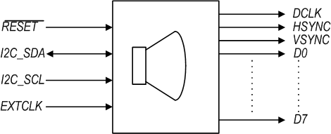
For the most part, CMOS cameras are controlled via the I2C interface (although I have come across devices that are controlled via the UART ). I2C is used to configure various parameters, such as: resolution, color gamma, output data format, etc.
The EXTCLK output is the clocking of the camera that needs to be provided from the outside. DCLK is a strobe signal, on the leading or trailing edge of which data is recorded on the camera data bus (for example, data bytes of one pixel of the matrix, or data bytes of "half-pixel" if the camera operates in RGB565 mode). HSYNC is a horizontal synchronization signal indicating the beginning of a new line, and VSYNC is a synchronization signal whose active level indicates the beginning of a new frame. Conclusions D0..D7 - data bus; As a rule, in such cameras it is eight-bit.
Now more about the synchronization signals.
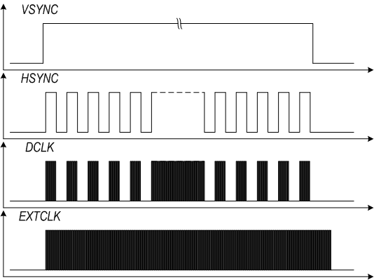
The graphs show that the camera is configured to activate the DCLK signal only during the active HSYNC phase (this is exactly what interests us, the clock signal during the “line feed” period is not interesting for us). If the camera is configured for a resolution of 320x240, then 320 DCLK pulses fit into the period of each HSYNC pulse, and 240 HSYNC during the VSYNC period.
When you increase the scale, we see what is happening on the data bus.
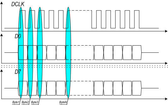
On the leading edge (in this case), a byte is removed from the data bus, which can be sent directly to the display for display, or “added” to a buffer for further processing.
In theory, everything is more or less clear, now about the DCMI interface of the STM32 microcontroller.
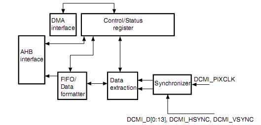
The DCMI interface is able to work with a data bus with a width of up to 14 bits, it supports both hardware and software synchronization, as well as data formats: YCbCr, RGB and JPEG.
In addition, DCMI contains a FIFO buffer, it has the ability to configure interrupts (including filling the data register) and setting up work via DMA .
Interrupts from DCMI can be triggered when the following conditions occur : line termination, frame termination, receiving buffer overflow, detection of a synchronization error (during internal synchronization).
The absence of a special camera clock output introduced me to some surprise. I do not know for what reasons the developers of SGS Microelectronics refused it, but for me, it would be very convenient to have, for example, a tunable clock source.
Personally, I used a general-purpose timer-counter, switched on in the PWM mode to generate a 4 MHz square wave. Of course, I won’t get a big FPS, but I’ll just make a reservation - the display I use is not connected to the FSMC , so the longest function in the whole circuit is the LCD display function, therefore, at a higher frequency, the display is disrupted . Therefore, before unloading, I turn off the timer, and after it - I turn on the timer again.
The DCMI hardware module contains, in addition to the data register, ten control / status registers. These are: control register ( DCMI_CR ), status register ( DCMI_SR ), interrupt status register ( DCMI_RIS ), interrupt enable register ( DCMI_IER ), interrupt mask register ( DCMI_MIS ), interrupt flag reset register ( DCMI_ICR ), internal synchronization code register ( DCMI_ESCR ) , the internal synchronization code mask reset register ( DCMI_ESUR ), the register of starting values when capturing a part of the frame ( DCMI_CWSTRT ) and the fragment fragment size register in CropWindow mode ( DCMI_CWSIZE ). And, of course, the data register is DCMI_DR .
In this case, the registers related to the capture of part of the frame and internal synchronization do not interest us. I also decided to leave the interrupts so far, so the only thing worth considering in more detail is the DCMI_CR control register and the DCMI_SR status register .
The control register allows us to fully customize the format of interaction with the camera: the size of the data bus, the active levels of the HSYNC and VSYNC lines , etc.
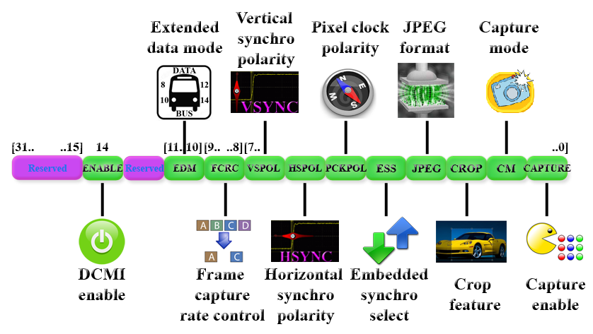
In order. The ENABLE bit - needless to say, the inclusion of the interface in the work. EDM field ( extended data mode ) - data bus size; The tire of my camera is eight-bit, so this field should be set to the value “00”. The FCRC ( frame capture rate control ) field allows you to adjust the FPC a bit: 00 — all incoming frames are captured, 01 is every second frame, 10 is every fourth. The VSPOL and HSPOL bits are the active levels of frame and line synchronization lines. Active levels are ignored and data are not captured during active periods, this should be taken into account. PCKPOL - bit of active pixel strobe level - on which edge of the signal to read data from the bus: front or back. ESS is the bit for selecting the synchronization method: external or internal. JPEG — select incoming data format — compressed or not. CROP - bit for selecting the frame fragment capture ( crop window ). If this bit is set to one, the interface will capture the data in the window defined by the values in the DCMI_CWSTRT and DCMI_CWSIZE registers .
So, set up.
Since I am used to using the standard periphery library from ST (although I never use it in the first iterations of working with the new periphery, until I dig into the registers with "pens"), I’ll bring up the settings using the library.
void DCMIInitialRoutine(void) { DCMI_InitTypeDef DCMI_CamType; DCMI_DeInit(); DCMI_CamType.DCMI_CaptureMode = DCMI_CaptureMode_Continuous; DCMI_CamType.DCMI_CaptureRate = DCMI_CaptureRate_All_Frame; DCMI_CamType.DCMI_ExtendedDataMode = DCMI_ExtendedDataMode_8b; DCMI_CamType.DCMI_SynchroMode = DCMI_SynchroMode_Hardware; DCMI_Init(&DCMI_CamType); DCMI_CaptureCmd(ENABLE); DCMI_Cmd(ENABLE); return; } Actually, for my needs, it was possible not to touch a single bit in the DCMI_CR register — by default, they were reset — except for the CAPTURE and ENABLE bits.
The interface is configured and ready to go. After the clock signal is sent to the camera, the interface will begin to accept the data we need to process.
The task to start with I set myself as simple as possible - to display the image on the display, so that the data processing will be minimal.
The status register DCMI_SR will help us in timely reading of data from the receiving buffer.
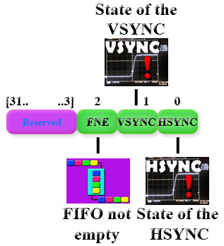
A very meager number of bits is available for reading - only three. The HSYNC and VSYNC bits indicate the status of the corresponding lines: active phase, or line feed; The most interesting is the FNE bit. He tells us to fill the buffer with data. Or not filling.
Checking in the constant cycle the state of the FNE bit in the DCMI_SR , we learn about the arrival of data in the receiving thirty-two-bit buffer. In my case, the data will be located as follows:
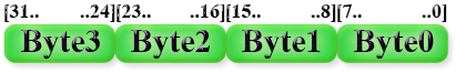
When setting the FNE bit in the status register DCMI_SR , the receiving buffer will contain four bytes, the data of two adjacent pixels: Byte0 and Byte1 - 16 bits of pixel n , and Byte2 and Byte3 - 16 bits of pixel n + 1 . I just need to combine them and send them for display on the display. So, this is how the main loop looks like:
while (1) { while ((DCMI_GetFlagStatus(DCMI_FLAG_FNE)) == RESET); //Waiting for the buffer TIM_Cmd(TIM3, DISABLE); //Disable CAM clock cam_grab = (DCMI->DR); //Reading buffer SendDataByte_LCD (cam_grab); cam_grab = (DCMI->DR)>>16; //Reading 2nd part of the buffer SendDataByte_LCD (cam_grab); TIM_Cmd(TIM3, ENABLE); //Enable CAM clock again } That is, I am waiting for the FNE bit in the DCMI_SR status register to be set , and after that, I unload 16 bits of data into the display in two steps .
At this point, I would like to come to a logical conclusion, but it was not there.
After flashing and restarting the MK on the display, I saw ... no, I saw my very own familiar physique, but in black and blue shades. Red and green colors were completely absent.
After a brief clash with the debager, the following was discovered: the interface data register contained only 16 data bits of a single pixel, with the lower 8 bits located at Byte0 (see figure above), and the older ones at Byte2 . The spaces Byte1 and Byte3 were empty. Until now, I did not understand where such a discrepancy is from the documentation of reality, and, perhaps, I will contact STM.
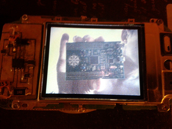
As a result, it was possible to obtain an image from the camera using the DCMI interface, although not without some difficulties. In the picture I bring a photo of the display on which the image of the STM32F3Discovery demo boards from my camera was displayed.
And here is what we will see on the pins of EXTCLK , PIXCK , HSYNC and VSYNC , if we connect a logic analyzer.
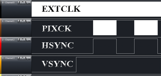
Everything looks exactly as expected: 240 HSYNC pulses fit in the duration of one VSYNC , 320 PIXCK - in one HSYNC . In the active phase of the HSYNC, the camera does not issue PIXCK signals - exactly as it was configured.
Generally speaking, the interface has somewhat disappointed me. The lack of a “regular” leg of the clocking of the camera, the absence of more or less interesting built-in chips (what about the hardware JPEG encoder?), And even dancing with a tambourine around a half FIFO ...
While organizing the work with the camera on the PIXCK , HSYNC and VSYNC interrupts, I didn’t have as much smut as I had while working with the camera using hardware DCMI .
Nevertheless, in the near future I will try to capture the frame, compress it in JPEG , and try to write a picture on the SD card.
Ps. Just in case, I give a link to the project for Code :: Blocks - it will suddenly come in handy to someone.
www.dropbox.com/sh/nfjdwqsdzlr7djm/9v2mQM8uYV
Source: https://habr.com/ru/post/186980/
All Articles