OPA Amplifier style
The article consists of 2 blocks:
1. Select the rail-to-rail input output (RRIO) of the operational amplifier for a wide range of applications.
And for geeks:
2. Create your own amp. Example.
Goal 1. First block
When creating a powerful amplifier for the transceiver , as well as an amplifier for the SubAMP series subwoofers , the question of measuring the voltage tightly between the power shelves arose. Namely, for example, we need to measure the current on a small-signal shunt sensor at a high positive potential of the power source, i.e. make High Side Current Sense. Namely, at the very plus, and the power of the operational amplifiers should not exceed it.
')
There are already ready current sensors, but we are perverted, we want cheap and original.
With earth measurements, everything is clear; there is a bunch of especially opamp amplifiers designed for this, such as lm124 (lm324), 2904, comparators 199, 139, 311 and the like with a p-channel differential pair at the input. Older tl07x and 08x type audiooperations, jrc4558, ne5532 have the same input p-pair for preferred operation near the ground / minus power supply of the operational amplifier.
But those who know it are well known that such a pair cannot measure signals close to a positive self-supply due to the voltage reserve necessary for the operation of current mirrors. In addition, p-channel transistors are less high-frequency. The inclusion of an opera with an n-channel pair at the input saves, but this is not a complete way out of our situation. For full kosher, in order to work with any signal level near minus and plus the power supply shelves of the operational amplifier, you need to use the rail-to-rail input structure. And in order to make it really good, you need to use this chip in input and output, i.e. Use RRIO OPA -rail-to-rail input output. There is another name for zamanuhi -beyond the rail OPAmp.
The N-channel pair within most op-amps ranges from just above the minimum to slightly above the power maximum (but not always), and the p-channel pair from just below the maximum to just below the minimum. As a result, combining them tokuko, we have a complete overlap on the input not only of the entire power supply bus of the operational amplifier, but also by about 0.2-0.5V beyond its limits in both directions, until the protective stops on the legs of the micrush are triggered.
It was not possible to find n-channel input amplifiers with a swoop. Posherstiv still managed to dig at a cursory examination of the ancient AD826 and LM360 / 361, and besides, they do not rail on the entrance. In general, disappointed. And this, as always with us, leads to the creation of something of our own (see Goal 2).
But then they immediately ran into the district of the opera. But we are pervert freaks, and this is not enough for us. Many scanned rail to rail amplifiers had a lot of flaws. If you even look at the official charts in datasheets, then everything gets worse. For many, with a large signal, itlays their ears on the front by clicking after exiting the power shelves, on the so-called restoration. This byak is found in very many even expensive operas, but you want something linear and correct. And for some, even the fronts of the rectangle are transmitted by a broken line. This is no good at all.
Also, not everything is nice with load capacity and input currents / drifts. A truly rail-to-rail structure is rarely found. Even from the expensive AD operas, almost everyone didn’t like it, then they had one, then another, and the price was high.
I had to sit and pick, which of the RRIO OPA have tolerable parameters for a wide and high-quality application. Oddly enough, normal was not enough. And they were selected solely on datasheets, and even there it’s full of glitches. Not to mention the real work, in it all the incidents manifest themselves in full force.
Below is a list of high-quality operational amplifiers with comments that are, in our opinion, worthy of attention for rail-to-rail applications, and it will be supplemented in the course of pushing them.
Preamble to goal 2.
When analyzing a huge heap, datasheets noticed an interesting point: the more symmetrically and more beautiful the schematic structure of the operational amplifier looks, the more correct, predictable and similarly more beautiful its parameters. As well as parameters at different power edges, restrictions and loads are obtained symmetrical and beautiful, understandable from the graphs and behavior.
For example, when you look at it
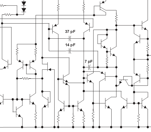
What is in my head immediately appears? That's right, my eyes would not see him, and even on a sober head. This is a piece of one widely known opera.
And it is already nice to see this, and the parameters are quite good. This is AD8614_8644.

And what to do if your hands itch?
Right!
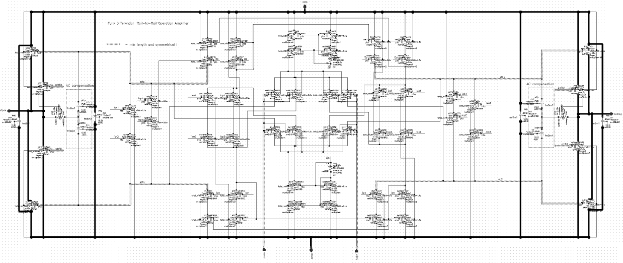
I could not resist and decided to make a dream operational amplifier, and not just rail to rail, but a fully differential differential input and output, such a high-quality operational amplifier of wide application according to the rules of microcircuit design .
Such amplifiers can be used both as ordinary single-output OPA (OA), without locking 1 of the outputs, and as normal diff. amplifiers for almost all modern paths of analog technology. Fully differential structure is now increasingly needed even in conventional signal processing, not to mention the ADC and DAC, which almost all have full-fledged diff. structure. This type of signal transmission allows you to partially eliminate tire interference and optimize current transmission and current flow. In the end, USB, SATA, PCIE, as well as all the RAM that I saw, and high-speed buses in computers and servers, have a differential structure. Well, or two-phase, the sound and light of friends. Differential improvement applies to all electrical systems, analog and digital. After all, except for currents and voltages there is nothing.
Further only electronic pornography goes.
As in good digital technology, it is extremely important to have a high-quality clock (time) support, so here in analog technology it is important to have sources of stable current and / or voltage that are not affected by different influences . At least one thing. Another can be done with this .
First, he created a stable temperature-compensated source of stable voltage — BandGap in everyday life, a so-called voltage source with a range gap, I mean a stabilizer 1v with voltage kopecks compensated in some temperature region of one sailing bysailing to another.
There is nothing complicated there, it is enough to remake it from the known solutions and finish it for our needs. Schemes roll in shared Internet.
The whole amplifier is powered from it through current multitranslators and mirrors. Its stability and noise determine the work and for the most part the temperature stability of the entire amplifier as a whole.
Naturally, this version of BandGap was investigated in a wide temperature & wide range and showed good stability. Now you can really rely on it.
It turned out this scheme. As they say, the face is terrible, but kind inside. But it is difficult to simplify.
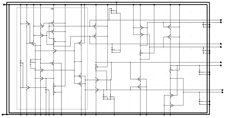
It contains some heap of current translators for breeding and feeding the amuser and the BandGap element itself (highlighted by a dotted line).
Current multipliers and repeaters in stock.
Maybe in the following articles I will tell you what and how it works in these amplifiers, and what elements are needed for.
Then I calculated the structure of the input fully differential cascade with minimized noise and a rail-to-rail input, and with a fully symmetrical structure.
To minimize the noise, large transistors and long channel lengths are used. Although the length of the field-effect transistor channel reduces its gain (steepness for correctness), it reduces the potential gradient along the length of the transistor, which also reduces the likelihood of pop corn mud noise and simply facilitates the operation of the transistor.
This is similar to a matrix in a camera, where large large pixels with a not large resolution of a sprinkled matrix, say, 3Mpix, give better image quality than small noisy specks of dust in any 7-14 Mpix camera. I have not seen one that is not very noisy with a small matrix size, and with a wild resolution in it.
And with large pixels in the top prof. matrices, and not really, the image acquires pixel-by-pixel detailing. What can not be said about the modern multi-megapixel soap. I still do not understand why the camera is 14Mpix, if everything is still blurry in the final photo. I come to the conclusion that the correct is not the size of the image resolution (this is just the amount that can be increased), but the size of the pixel itself, its dimensions. A pixel in modern cameras is essentially a transistor, more precisely, a phototransistor, but this does not change the essence. Let's go further.
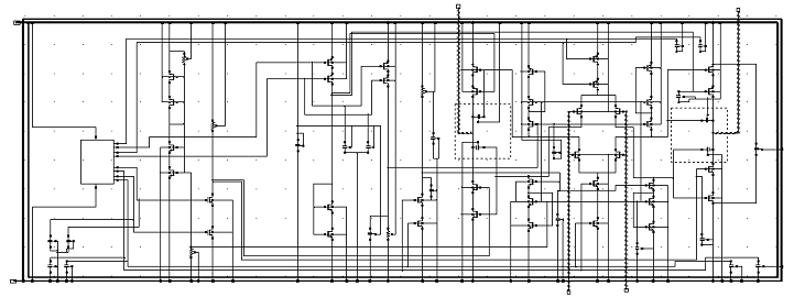
Then he estimated and realized the structure of the pre-terminal cascade with the balance of currents and the terminal fully differential cascade. A single frequency band turned out in the region of 50 megahertz, and it is easy at that, even on large 180nm transistors. For the stability of this band and the phase margin, topological protective rings, shields and internal pockets are provided in the topology.

In the process, we had to study how best to do folded cascode and just good cascode current sources, what is their stability and how to make high-quality mirrors and multichannel correct stable current transformers (cascodes, resistors in the sources).
As for the terminator, there wasn’t much fear, there are no switched capacitor solutions, class I , voltage additives E, and other modern enhancements. Only Terry Class AB. For the power supply, this amp is 3.0-3.6V, since it was made on a 3.3-volt LV library. The other was not at hand. And so, there are 140V of LTC6090 opera in the world, and, possibly, more high-voltage ones. Allowable stress is a problem only of the libraries from which the device is made. Although you can always stir up the voltage add-on or conversion, if not enough springs.
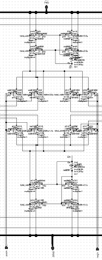
The complete diagram of the core of the amplifier without the weight and the necessary garden is given below.
Testing took place on the torture table, which for ethical reasons is not shown here. In general, it is a variety of ideal sources / loads / effects that you can imagine only in a nightmare. While he endured everything, he was made in the chip, and confirmed his parameters.
I checked the layout on numerous parameters, for resistance to technological variations and probabilistic variations. That is not laziness, not laziness, when you do for yourself and with love.
Each block was tested separately and in the system before inserting it into a block above it.
Up to this point, the layout was deliberately pulled up to the necessary input modes using external sources. Everything was set up according to the most important principle — to obtain the most needed readings without general feedback, that is, to obtain the structure initially as linear as possible, and only then introduce external feedback , for research and final measurements. I think no one will argue here, this is the postulate of all linear electronics and analog circuitry.
Prior to that, these toilets were writing until it began to follow the main principles of design. Accuracy, beauty and conciseness are our best friends. And everything starts to work nicely, because it becomes clear. The reliability of systems increases, because you see every step, it is clear and understandable.
And finally, he covered him with the third entrance of the CMFB, when everything else began to work perfectly. Then VCL zaklokotal as it should, right already takes the joy!
Who does not know, cmfb is a common mode feedback, settling all the outputs of the operational amplifier relative to the support given to the third input CM. This is such a negative feedback for the middle point of the amplifier. Otherwise, how will he know about which line to give a swing at the outputs of the amplifier?
This is the very third input with a bypassing air-conditioner, which is usually needed for the common line of all devices of the path to the amplifier, after, and himself. Something like that
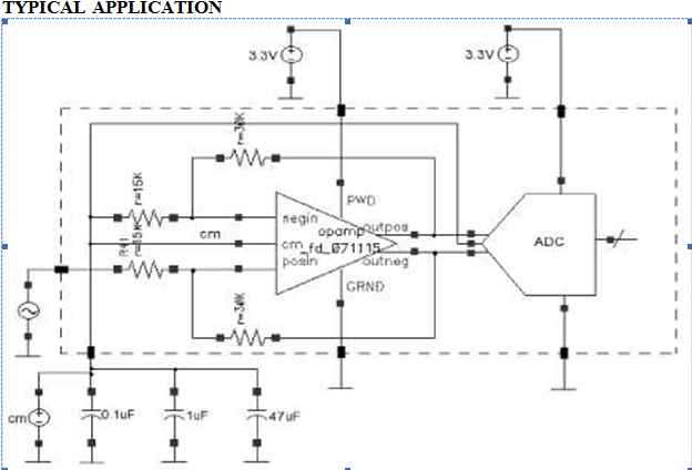
The level of the common point (or, in a different way, virtual ground, midpoint, common mode) is usually half of the power shelves, but it may be different. And there can be not only potential, but also current, what a difference to us is the voltage, this is the result of the current on the resistor, the effect of the current, and we always get the voltage when we want.
Here is a system of continious time voltage CMFB of this amplifier.

It connects to its two outputs and its reputation affects the erogenous point in the form of two inputs of a parallel amplifier connected to the output stage. Something like familiar shunt regulator TL432 series.
CMFB is essentially an amplifier in an amplifier, a second loop, which should be faster than the main circuit to provide global stability to the amplifier. By the way, everything I write about here is a thing of many years ago, I wanted to bring everything together, and to have a look, to remember. Such an express overview of some of the necessary things.
Results of goal 2
The parameters obtained in this library are not super-duper, but stable, almost the same that I wanted to get, besides, they can always be multiplied to high powers / currents. Yes, I forgot to say, this opera was planned for internal finishing works in a microcircuit, not for external. For ekstalki made others and separately. They are briefly described below.
Brief parameters of the resulting OPA.
FEATURES OPA:
Fully Differential Opamp
Supply Voltage Range: 3 V ... 3.6 V
Unity Gain-Bandwidth: 54 MHz
Slew Rate: 129 V / us
Output Current: up to 1 mA sink / source @each channel
DC Voltage Offset: 1.2 mV max
Supply Current: 0.87 mA
Open Loop Gain: 74 dB
This is enough for us to work inside the microcircuits, and he was born for this. Output Impedance it in the region of 500 Ohm does not confuse the microcircuit neighbors. For especially zealous there are drivers with low impedance.
Intracircuit electronic products, as it turned out in practice, are easy to do, he himself was surprised, I’ll bring something else to heaps.
Nano-current 1.8 and 3.3-volt devices, as well as switching cap systems, track-hold, ADC, sc comparators, delay, eq, linear phase filters, PGA, DAC, charge pump, vco-pll, mixers, rf pa, limiting amp , multiphase pwm and a lot of rubbish. Everything basically turned out to be simple.
To throw the signal out, to pump the pad of the PAD chip and the external load capacity, a sophisticated version of this amplifier was invented, as well as special analog buffers based on it.
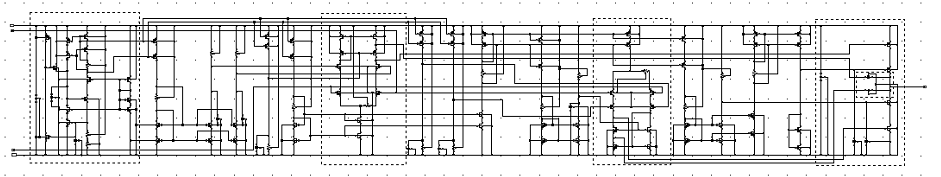
Here is even wiser, scary kids.

These buffers are not all very beautiful, they were made before the aspen and clearly delirious. They have a band in the region of 400 MHZ and stable work on the capacitive load.
In general, analog technology is not as scary as it is painted.
PDF of the rest of the ready devices I will attach if anyone needs it.
Ps. Thanks for attention.
Appendix: homemade simple operational amplifier
diybass.com/wp-content/uploads/2013/FD-RRIO-OPA.pdf
1. Select the rail-to-rail input output (RRIO) of the operational amplifier for a wide range of applications.
And for geeks:
2. Create your own amp. Example.
Goal 1. First block
Choosing the right rail-to-rail input output (RRIO) and low-cost opamp for a wide range of ready-made devices.
When creating a powerful amplifier for the transceiver , as well as an amplifier for the SubAMP series subwoofers , the question of measuring the voltage tightly between the power shelves arose. Namely, for example, we need to measure the current on a small-signal shunt sensor at a high positive potential of the power source, i.e. make High Side Current Sense. Namely, at the very plus, and the power of the operational amplifiers should not exceed it.
')
There are already ready current sensors, but we are perverted, we want cheap and original.
With earth measurements, everything is clear; there is a bunch of especially opamp amplifiers designed for this, such as lm124 (lm324), 2904, comparators 199, 139, 311 and the like with a p-channel differential pair at the input. Older tl07x and 08x type audiooperations, jrc4558, ne5532 have the same input p-pair for preferred operation near the ground / minus power supply of the operational amplifier.
But those who know it are well known that such a pair cannot measure signals close to a positive self-supply due to the voltage reserve necessary for the operation of current mirrors. In addition, p-channel transistors are less high-frequency. The inclusion of an opera with an n-channel pair at the input saves, but this is not a complete way out of our situation. For full kosher, in order to work with any signal level near minus and plus the power supply shelves of the operational amplifier, you need to use the rail-to-rail input structure. And in order to make it really good, you need to use this chip in input and output, i.e. Use RRIO OPA -rail-to-rail input output. There is another name for zamanuhi -beyond the rail OPAmp.
How is the rail-to-rail structure made? OPA inside
The N-channel pair within most op-amps ranges from just above the minimum to slightly above the power maximum (but not always), and the p-channel pair from just below the maximum to just below the minimum. As a result, combining them tokuko, we have a complete overlap on the input not only of the entire power supply bus of the operational amplifier, but also by about 0.2-0.5V beyond its limits in both directions, until the protective stops on the legs of the micrush are triggered.
It was not possible to find n-channel input amplifiers with a swoop. Posherstiv still managed to dig at a cursory examination of the ancient AD826 and LM360 / 361, and besides, they do not rail on the entrance. In general, disappointed. And this, as always with us, leads to the creation of something of our own (see Goal 2).
But then they immediately ran into the district of the opera. But we are pervert freaks, and this is not enough for us. Many scanned rail to rail amplifiers had a lot of flaws. If you even look at the official charts in datasheets, then everything gets worse. For many, with a large signal, it
Also, not everything is nice with load capacity and input currents / drifts. A truly rail-to-rail structure is rarely found. Even from the expensive AD operas, almost everyone didn’t like it, then they had one, then another, and the price was high.
I had to sit and pick, which of the RRIO OPA have tolerable parameters for a wide and high-quality application. Oddly enough, normal was not enough. And they were selected solely on datasheets, and even there it’s full of glitches. Not to mention the real work, in it all the incidents manifest themselves in full force.
Total goal 1 . Selection of a ready-made RRIO operational amplifier for everyday needs.
Below is a list of high-quality operational amplifiers with comments that are, in our opinion, worthy of attention for rail-to-rail applications, and it will be supplemented in the course of pushing them.
Prispandoreno-prihabreno
Here is a list of true rail-to-rail input output (RRIO) and beyond-the-rail op-amps with a brief description of their advantages and disadvantages so that you can choose the best or quickly estimate what you need and then study it in detail in the datasheet.
LMV931,932 1.8-5V, all is well, but the power is low
LMV981,982 1.8-5V, shape forms, low power
NCS7101, 1.8-10V, similar to LMV931, better power
NCS2001,2002 0.9-5V, similar to LMV931
MC33201 / 2/4 0.9-12V, similar to LMV931, better power, Input Offset Voltage is large, approx. 10mV
LM7301- 1.8 ... 32V, crooked rectangle, single only
ADA4092 3-30V, serifs on the rectangles
MC33201 1.8 ... 12V, crooked rectangle
AD8614 / 8644 5-18V, unprotected 70mA out
Preamble to goal 2.
Beauty will save the chips
When analyzing a huge heap, datasheets noticed an interesting point: the more symmetrically and more beautiful the schematic structure of the operational amplifier looks, the more correct, predictable and similarly more beautiful its parameters. As well as parameters at different power edges, restrictions and loads are obtained symmetrical and beautiful, understandable from the graphs and behavior.
For example, when you look at it
What is in my head immediately appears? That's right, my eyes would not see him, and even on a sober head. This is a piece of one widely known opera.
And it is already nice to see this, and the parameters are quite good. This is AD8614_8644.
Goal 2. The second block . Create your dream operational amplifier with the right parameters.
And what to do if your hands itch?
Right!
Designing your own rail to rail IO amplifier.
I could not resist and decided to make a dream operational amplifier, and not just rail to rail, but a fully differential differential input and output, such a high-quality operational amplifier of wide application according to the rules of microcircuit design .
Fully differential amplifiers. Fully differential OPA
Such amplifiers can be used both as ordinary single-output OPA (OA), without locking 1 of the outputs, and as normal diff. amplifiers for almost all modern paths of analog technology. Fully differential structure is now increasingly needed even in conventional signal processing, not to mention the ADC and DAC, which almost all have full-fledged diff. structure. This type of signal transmission allows you to partially eliminate tire interference and optimize current transmission and current flow. In the end, USB, SATA, PCIE, as well as all the RAM that I saw, and high-speed buses in computers and servers, have a differential structure. Well, or two-phase, the sound and light of friends. Differential improvement applies to all electrical systems, analog and digital. After all, except for currents and voltages there is nothing.
Further only electronic pornography goes.
Putting it in pieces. Support
As in good digital technology, it is extremely important to have a high-quality clock (time) support, so here in analog technology it is important to have sources of stable current and / or voltage that are not affected by different influences . At least one thing. Another can be done with this .
First, he created a stable temperature-compensated source of stable voltage — BandGap in everyday life, a so-called voltage source with a range gap, I mean a stabilizer 1v with voltage kopecks compensated in some temperature region of one sailing by
There is nothing complicated there, it is enough to remake it from the known solutions and finish it for our needs. Schemes roll in shared Internet.
The whole amplifier is powered from it through current multitranslators and mirrors. Its stability and noise determine the work and for the most part the temperature stability of the entire amplifier as a whole.
Naturally, this version of BandGap was investigated in a wide temperature & wide range and showed good stability. Now you can really rely on it.
It turned out this scheme. As they say, the face is terrible, but kind inside. But it is difficult to simplify.
It contains some heap of current translators for breeding and feeding the amuser and the BandGap element itself (highlighted by a dotted line).
Current multipliers and repeaters in stock.
Maybe in the following articles I will tell you what and how it works in these amplifiers, and what elements are needed for.
Inputs for fully differential rail-to-rail amplifier
Then I calculated the structure of the input fully differential cascade with minimized noise and a rail-to-rail input, and with a fully symmetrical structure.
To minimize the noise, large transistors and long channel lengths are used. Although the length of the field-effect transistor channel reduces its gain (steepness for correctness), it reduces the potential gradient along the length of the transistor, which also reduces the likelihood of pop corn mud noise and simply facilitates the operation of the transistor.
This is similar to a matrix in a camera, where large large pixels with a not large resolution of a sprinkled matrix, say, 3Mpix, give better image quality than small noisy specks of dust in any 7-14 Mpix camera. I have not seen one that is not very noisy with a small matrix size, and with a wild resolution in it.
And with large pixels in the top prof. matrices, and not really, the image acquires pixel-by-pixel detailing. What can not be said about the modern multi-megapixel soap. I still do not understand why the camera is 14Mpix, if everything is still blurry in the final photo. I come to the conclusion that the correct is not the size of the image resolution (this is just the amount that can be increased), but the size of the pixel itself, its dimensions. A pixel in modern cameras is essentially a transistor, more precisely, a phototransistor, but this does not change the essence. Let's go further.
2nd stage amp, csda / vcda-type schematics. Balanced Current Preamplifier
Then he estimated and realized the structure of the pre-terminal cascade with the balance of currents and the terminal fully differential cascade. A single frequency band turned out in the region of 50 megahertz, and it is easy at that, even on large 180nm transistors. For the stability of this band and the phase margin, topological protective rings, shields and internal pockets are provided in the topology.
In the process, we had to study how best to do folded cascode and just good cascode current sources, what is their stability and how to make high-quality mirrors and multichannel correct stable current transformers (cascodes, resistors in the sources).
Output stage DIY RRIO Amplifier. Output stages
As for the terminator, there wasn’t much fear, there are no switched capacitor solutions, class I , voltage additives E, and other modern enhancements. Only Terry Class AB. For the power supply, this amp is 3.0-3.6V, since it was made on a 3.3-volt LV library. The other was not at hand. And so, there are 140V of LTC6090 opera in the world, and, possibly, more high-voltage ones. Allowable stress is a problem only of the libraries from which the device is made. Although you can always stir up the voltage add-on or conversion, if not enough springs.
The complete diagram of the core of the amplifier without the weight and the necessary garden is given below.
Testing
Testing took place on the torture table, which for ethical reasons is not shown here. In general, it is a variety of ideal sources / loads / effects that you can imagine only in a nightmare. While he endured everything, he was made in the chip, and confirmed his parameters.
I checked the layout on numerous parameters, for resistance to technological variations and probabilistic variations. That is not laziness, not laziness, when you do for yourself and with love.
Each block was tested separately and in the system before inserting it into a block above it.
Natural principles of construction
Up to this point, the layout was deliberately pulled up to the necessary input modes using external sources. Everything was set up according to the most important principle — to obtain the most needed readings without general feedback, that is, to obtain the structure initially as linear as possible, and only then introduce external feedback , for research and final measurements. I think no one will argue here, this is the postulate of all linear electronics and analog circuitry.
Prior to that, these toilets were writing until it began to follow the main principles of design. Accuracy, beauty and conciseness are our best friends. And everything starts to work nicely, because it becomes clear. The reliability of systems increases, because you see every step, it is clear and understandable.
Common mode voltage feedback- CMFB for RRIO FD OPAmp
And finally, he covered him with the third entrance of the CMFB, when everything else began to work perfectly. Then VCL zaklokotal as it should, right already takes the joy!
Who does not know, cmfb is a common mode feedback, settling all the outputs of the operational amplifier relative to the support given to the third input CM. This is such a negative feedback for the middle point of the amplifier. Otherwise, how will he know about which line to give a swing at the outputs of the amplifier?
This is the very third input with a bypassing air-conditioner, which is usually needed for the common line of all devices of the path to the amplifier, after, and himself. Something like that
The level of the common point (or, in a different way, virtual ground, midpoint, common mode) is usually half of the power shelves, but it may be different. And there can be not only potential, but also current, what a difference to us is the voltage, this is the result of the current on the resistor, the effect of the current, and we always get the voltage when we want.
Here is a system of continious time voltage CMFB of this amplifier.
It connects to its two outputs and its reputation affects the erogenous point in the form of two inputs of a parallel amplifier connected to the output stage. Something like familiar shunt regulator TL432 series.
CMFB is essentially an amplifier in an amplifier, a second loop, which should be faster than the main circuit to provide global stability to the amplifier. By the way, everything I write about here is a thing of many years ago, I wanted to bring everything together, and to have a look, to remember. Such an express overview of some of the necessary things.
What did we get? And what can you get?
Results of goal 2
The parameters obtained in this library are not super-duper, but stable, almost the same that I wanted to get, besides, they can always be multiplied to high powers / currents. Yes, I forgot to say, this opera was planned for internal finishing works in a microcircuit, not for external. For ekstalki made others and separately. They are briefly described below.
Brief parameters of the resulting OPA.
FEATURES OPA:
Fully Differential Opamp
Supply Voltage Range: 3 V ... 3.6 V
Unity Gain-Bandwidth: 54 MHz
Slew Rate: 129 V / us
Output Current: up to 1 mA sink / source @each channel
DC Voltage Offset: 1.2 mV max
Supply Current: 0.87 mA
Open Loop Gain: 74 dB
This is enough for us to work inside the microcircuits, and he was born for this. Output Impedance it in the region of 500 Ohm does not confuse the microcircuit neighbors. For especially zealous there are drivers with low impedance.
Intracircuit electronic products, as it turned out in practice, are easy to do, he himself was surprised, I’ll bring something else to heaps.
Nano-current 1.8 and 3.3-volt devices, as well as switching cap systems, track-hold, ADC, sc comparators, delay, eq, linear phase filters, PGA, DAC, charge pump, vco-pll, mixers, rf pa, limiting amp , multiphase pwm and a lot of rubbish. Everything basically turned out to be simple.
Driving IC PADs
To throw the signal out, to pump the pad of the PAD chip and the external load capacity, a sophisticated version of this amplifier was invented, as well as special analog buffers based on it.
Here is even wiser, scary kids.
These buffers are not all very beautiful, they were made before the aspen and clearly delirious. They have a band in the region of 400 MHZ and stable work on the capacitive load.
In general, analog technology is not as scary as it is painted.
PDF of the rest of the ready devices I will attach if anyone needs it.
Ps. Thanks for attention.
Appendix: homemade simple operational amplifier
diybass.com/wp-content/uploads/2013/FD-RRIO-OPA.pdf
Source: https://habr.com/ru/post/186402/
All Articles