How to test electronics in production: an analysis of modern technology
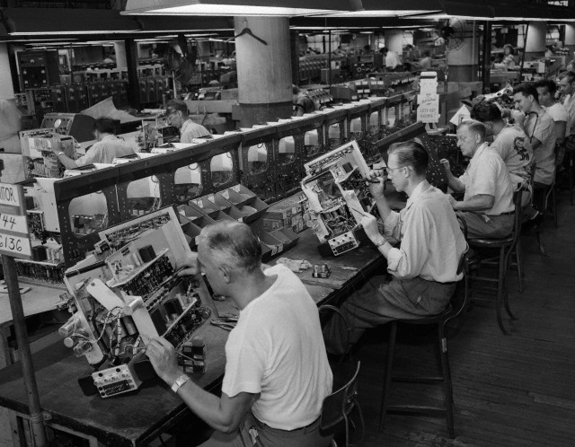
The final stage in the creation of an electronic product is mass production, it ultimately determines the quality of the device. The user will not be able to evaluate the ideal software and hardware platform of the new electronics, if the assembly line fails, therefore, functionality control and assembly testing are necessary stages of mass production.
Readers of this article will become familiar with the basic techniques and tasks of testing electronic devices and gain a general understanding of quality assurance in manufacturing. Special attention will be paid to the advantages and disadvantages of various testing methods.
Types of testing in production. Short review
In general, the process of preparing and testing an electronic product in production is as follows:
- Design and build a stand for firmware and testing using JTAG / ICT testing
- Development of a test system and parameters for quality control and production acceptance
- Automated or manual functionality check
Testing the device and its individual parts in the production process can be implemented on the basis of the following methods and technologies:
')
1. Visual automated control ( AOI , AXI ) is a preliminary quality check, which is used in any contract manufacturing, it takes place at different stages of the assembly of printed circuit boards, including using X-rays to check places that are invisible to the eye or standard optical systems.

In the photo: The printed circuit board passes visual automated control ( AOI ). According to the test results, the tester will receive data on detected defects. Source: Acculogic .
2. In-circuit testing ( ICT / FICT ) - checking connections and components on a printed circuit board, analyzing the electrical parameters of the entire circuit or its individual sections.
This method uses the contact of probes with the nodes of the assembled board: this can be either a stationary field of contacts (“bed of nails”, English - bed of nails), and “flying probes” (flying probe) or “flying matrices”. Often requires the use of complex and expensive equipment, technological training, manufacturing of special equipment.
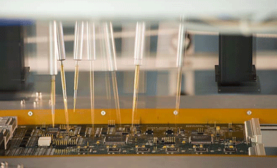
In the photo: testing of the circuit board by “flying probes” (flying probes).
Source: Acculogic .
3. Peripheral / Boundary Scan (boundary scan) - testing using JTAG. Based on the use of IEEE 1149 standard support chips.
4. Functional testing ( FCT ) - verification of assembled or partially assembled devices for the performance of a given functionality and for compliance with the parameters that are laid down in the specification for the device.
All of these techniques allow us to assess the quality of the electronics in the production process, but in some cases the device is tested only at the final stage. This so-called testing after final assembly ( EOL ) is a test of functionality and conformance with specifications. Not only quality is evaluated, but also the stability and reliability of the device. This analysis of electronics takes place using complex bench equipment that simulates the system as part of which the device under test operates. If according to the results of such a check, the reject rate exceeds the preliminary estimate, then the production technology is adjusted and the next trial batch of devices is launched. And so in several iterations.
In practice, the best results are shown by the methods used in the production process, i.e. functional and in-circuit testing, because they allow you to quickly obtain information and identify specific stages at which problems arise. This allows you to make adjustments to the production process before the final assembly of the device.
Let us consider these testing methods in more detail, from the general to the particular, starting with the analysis of the functionality of assembled or partially assembled devices and ending with the features of in-circuit testing of printed circuit boards.
Functional testing in production
Functional testing can be carried out both in manual and automatic mode. Naturally, in the preparation of test plans, manual labor is attempted to be minimized, leaving the operator only the connection / disconnection of the device, as well as the control of validity.
With the right approach, this technique is able to cover almost all the functionality of the device in record time. However, without the development of test software and the manufacture of special equipment is not enough.
Testing can be divided into testing the main parts of the device (processor, memory, other modules) and testing peripheral interfaces. To test the processor, a special program is created that automatically sets specific operating parameters, initializes all the device's microcircuits, polls them and, based on the results obtained, concludes that it is working. After the main parts are checked, the operating mode is switched on for each component part of the device and its functionality is checked. For example, to test Ethernet interfaces, the program alternately initializes each port, and if there are several, it sets temporary MAC and IP addresses, forwards packets, and analyzes the result.
The degree of product coverage tests is determined individually for each type of device based on the analysis of the electrical circuit, available for testing modules and interfaces.
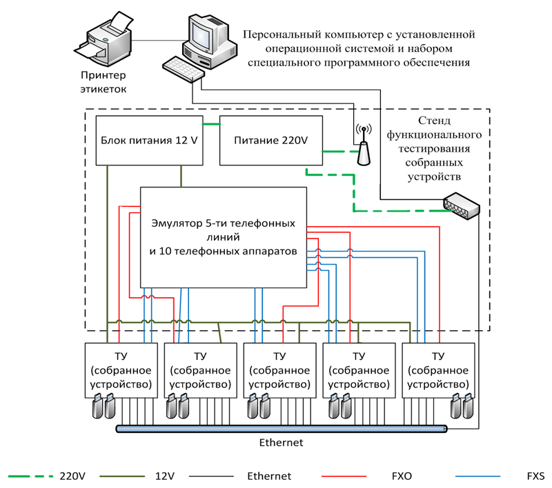
In the diagram: Stand functional testing assembled devices.
Above is a diagram of the stand of functional testing of assembled devices. It allows you to test five devices at the same time, consistently testing all the functionality of each. In the process, the firmware versions of individual modules are checked, and, if necessary, the firmware is updated with the latest version. After successfully passing the tests, the program provides the device with a MAC address, serial number and preset passwords.
Functional testing stands can include auxiliary software and hardware to personalize the device, remotely collect information about the devices under test, generate defect reports.
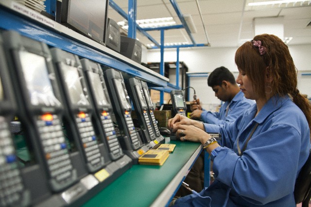
Pictured: Functional testing of assembled devices at a factory in Singapore.
The test results are displayed on the computer monitor, to the stand simultaneously.
seven instruments are connected.
The indisputable advantages of functional testing include the possibility of final firmware, checking and updating software versions of system modules, issuing personal data to a device using high-level protocols and high-speed interfaces.
Functional testing stands can be integrated into automated systems of an enterprise (production) and provide accounting and collection of statistical information from production sites and quality control departments.
The main disadvantages of this method of testing devices are the need to manufacture specialized tooling and writing software, as well as functional testing, unlike peripheral scanning, does not give an exact indication of defective circuits and component leads. But in most cases carrying out these works is justified due to the maximum coverage and short testing time.
Testing of electronic devices in the production method of peripheral scanning
Now we will consider the following testing methodology, which allows controlling the quality of installation and discarding devices before the functional testing stage. This is JTAG testing.
Tests for peripheral scanning (boundary-scan) can improve the quality of the developed devices and save costs at the stage of mass production. The main advantage of this technology is the ability to test devices with limited access to the leads of microcircuits in BGA, COB and QFP packages.
Recently, due to the large spread of the JTAG standard and, accordingly, of chips with its support, the method of peripheral scanning has become increasingly available.
Chip makers accompany their products with BSDL files that contain information about the architecture of peripheral scanning registers. Modern software tools for JTAG testing can automate the process using data schematics from CAD. All this simplifies the preparation and use of JTAG testing.
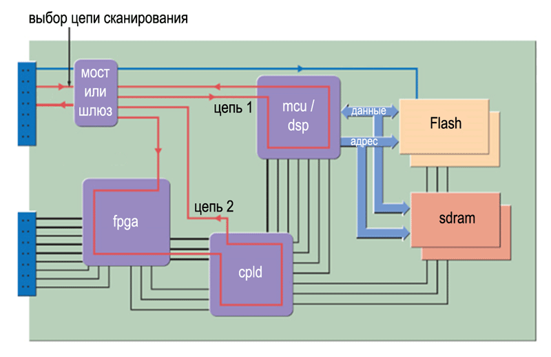
In the diagram: Example JTAG testing. Here you can see how you can check the components that are connected to the bus of the tested chip, but do not directly support the JTAG standard (for example, flash memory and SDRAM).
When designing electronic devices, preliminary preparation of the product circuit is required. At a minimum, this is the use of components that support the IEEE 1149.1 standard, the correct connection of these components, the output of JTAG ports to external contacts or connectors.
JTAG-testing allows you to identify "not damn" the inputs of digital circuits with different types of enclosures, including BGA, circuits, breaks, as well as non-working chips with digital interfaces. It is very important to identify all these defects, since if an untested board goes to the programming stage, problems may arise with the launch of memory and peripherals. It will be difficult to determine the cause of the problem: incorrect software settings or a mounting defect. JTAG testing can prevent this problem.
However, JTAG testing has its drawbacks. First, it is low productivity in comparison with functional testing. Secondly, the method is intended for testing digital electronics, respectively, the analog parts of the device are excluded. Third, it is important to keep in mind that JTAG testing only verifies the integrity of links, but not their quality. Impedance, parasitic capacitance, etc. - all these quality parameters can significantly affect the operation of high-speed circuits.
JTAG testing also has several other limitations:
- It is impossible to detect installation defects related to digital or analog elements that do not have JTAG support, and diagnostics of communication defects between them is also unavailable.
- It is not possible to perform functional tests or tests aimed at detecting faults that are a function of time.
- It is not possible to perform tests aimed at detecting such data bus defects as, for example, jitter, interference (crosstalk), interference, etc. (tests for the PCI bus).
But at the same time, JTAG testing has significant advantages. This is a deep analysis of the performance of microcircuits and modules for selective testing of electronic devices in an industrial lot. This is an important addition, and in some cases - the replacement of in-circuit testing with the help of a “bed of nails” or “flying probes”. JTAG allows you to optimize equipment for full testing or reduce the time for testing with an integrated approach when it is used in conjunction with other methods.
Also, as the requirements for miniaturization of electronic devices grow, JTAG testing reduces the size of a printed circuit board by avoiding the need to place groups of contact pads on it for in-circuit testing using the “bed of nails”.

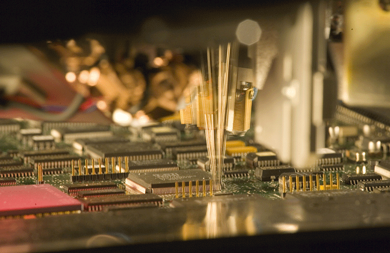
In the photo: In-circuit testing using the "bed of nails." Source: Spea .
In-Circuit Testing
Although peripheral scanning using JTAG technology is gaining increasing popularity, the classical method of in-circuit testing, which began to develop from the 70s - 80s of the 20th century, has been successfully used so far.
In-Circuit Testing is a technology for testing individual components on the board or circuit fragments using special equipment (ICT stations) and accessories (needle adapter). Thanks to this testing technique, it is possible to analyze individual components and analog parts of circuits. And also successfully applied in large-scale production. Those. in cases where other modern technologies fail.
Conventionally, in-circuit testing can be divided into analog and digital. With analog in-circuit testing, the following characteristics are usually checked:
- the presence of short circuits and breaks;
- ratings of discrete components (resistors, capacitors, inductances, discrete semiconductor devices);
- availability and correct installation of microcircuits.
This testing method allows you to detect a large number of assembly defects, so analog in-circuit testing is often called an analysis of manufacturing defects.
With digital in-circuit testing, digital chips are checked for compliance with the truth table.
Since this technology is based on the physical contact of the needles with the contacts of the tested components, a number of difficulties arise when implementing this approach in testing.
The constant miniaturization of components leads, among other things, to a reduction in the physical dimensions of the contact pads and their movement under the housing. Also in multilayer printed circuit boards, a significant number of connections are implemented in the inner layers. All this leads to the need to output contact pads for the ICT adapter to one of the sides of the board, which in turn causes an increase in its dimensions and complicates their routing, and often, in the case of high-frequency buses, this is impossible in principle.
One of the solutions to these problems is to use the test method of "flying probes" or "flying matrices." This approach avoids the need to output special contact pads for testing, but significantly increases the inspection time, which is a significant limitation for mass production.
In the photo: another example of testing the circuit board with “flying probes”. Source: Acculogic .
Another and, probably, the main way to optimize the in-circuit testing technology, without prejudice to the density of test coverage of a printed circuit board and by the time of testing, is an integrated approach, which consists in combining classical ICT testing with JTAG testing. Such an approach, when pre-calculating the coverage of a printed circuit board by tests and distributing them between JTAG and ICT, allows minimizing the number of sites for ICT needles and, accordingly, simplifies and cheapens the testable fee. The use of such methods requires an appropriate approach when designing an electronic device, analyzing the testability of electrical circuits, their adjustment.

PrintScreen: sample test coverage report. Source: Acculogic .
findings
Thus, we can form the main criteria that determine the choice of testing methodology:
- The scale of production.
- The complexity of the product.
- The presence of special requirements for quality (example: electronics responsible use).
For example, for relatively simple devices in small batches, it is sufficient to use functional testing, and for simple electronics in large series - in-circuit testing, since It provides maximum speed. For testing digital electronics with support for JTAG technology, peripheral scanning is the optimal choice; it allows you to debug the production process and correct it at an early stage.
When planning mass production, it is necessary to take into account the performance of all test methods, and, accordingly, such a combination of them in order to get the minimum time to test a single device with maximum test coverage. For example, in many cases, testing with a “bed of nails” and peripheral scanning are preferred methods compared to functional testing and testing with “flying probes” in terms of speed characteristics.
Accordingly, it is the integrated testing of electronics in production , i.e. The combination of various technologies in a competent proportion today is the best option for checking and analyzing quality. For this reason, a predesign analysis of testability and test coverage comes to the fore. It allows you to initially plan and justify the applicability and degree of use of the approaches described above in each specific project.
& nbsp
[!?] Questions and comments are welcome. They will be answered by the maintenance engineer of the electronics design center Promwad.
Source: https://habr.com/ru/post/185356/
All Articles