Perform transactions on the PCI bus. Implementation on VHDL
Not so long ago, I asked about the mechanism for polling PCI devices. After that I got a job, completed the test task, and I asked exactly about him, and safely forgot about him. But recently they gave out a new project and had to remember everything, at the same time and decided to write here.
There are quite a few transactions on the PCI bus; only the following will be described in this topic:
When making transactions, there are 2 options:
As it already happened, when considering the PCI bus, I will call the master device a master (Master), the slave - a target (Target).
This article deals only with transactions when the master is the south bridge, since transactions when the master is a device connected to the PCI bus deserves a separate article.
And so, to work with the bus, we need the following signals:
')
clk (Clock) - provides synchronization of all transactions on a PCI, and is also an input for each PCI device.
AD (Address and Data) - multiplexing address bus and data.
IDSEL (Initialization Device Select) is a selection of an initialization device, used to select a chip during a read configuration and write transaction.
CBE (Bus Command and Byte Enables) - bus commands and byte resolution.
FRAME (Frame) - the signal is issued by the master at the beginning of the transaction and determines its duration. For single-phase FRAME transactions, one cycle always lasts. In multiphase transactions, FRAME is removed one cycle before the completion of the transaction.
IRDY (Initiator Ready) - a signal of readiness of the master. It indicates that the wizard is ready to complete the current data phase.
TRDY (Target Ready) - a target readiness signal indicating that the target is ready to complete the current data phase.
STOP (Stop) - this signal is given by the target, if it wants to stop the current transaction.
PAR (Parity) - parity control on lines AD and CBE.
RST (Reset) - a reset signal. It is asynchronous.
DEVSEL (Device Select) - the device selection signal.
Before you start working with any device, you need to initialize it. Therefore, we consider the features of the configuration transactions.
Format of the configuration register:

The minimum set of registers:
For memory areas and port descriptions are different:
The size of the areas is calculated as follows. 0xFFFFFFFF is written to the BAR. Further, the value is read from BAR, and subtracted from 0xFFFFFFFF. The result is the size of the area. The unit in the low bit is not counted.
The master sets the device address on the AD bus, the command to be executed on the CBE bus, sets the FRAME signal to 0 and the IRDY signal to 0. Next, the master waits from the target — setting it to TRDY and DEVSEL signals. Also, the target puts the requested data onto the AD bus. Data is considered valid when IRDY, TRDY and DEVSEL are equal to the logical zero level.
To access the FPGA outputs, special components are required: I / O buffers for working with the Z-state.
So, for the AD bus, the connection will look like this:
Where,
For the rest of the signals in the same way, I will not quote, so as not to overload the article.
As I wrote above, at the beginning of a transaction, when the address is set on the AD bus, the FRAME signal is always zero. Below is the code that generates the AdrPhASE signal, during which you need to latch the address bus and the command bus for subsequent work. In fact, the AdrPhASE signal is nothing more than the selection of the falling edge of the FRAME signal, which uniquely identifies the beginning of the transaction.
Further, the operation of the entire device can be described using an automaton.
To understand the above written, I will give the possible commands transmitted via the CBE bus.
Each team has its own state machine. Switching to it depends on the current state of the CBE bus and the AD bus for accessing memory and I / O ports. The exit to the initial state is performed by the arrival of the IRDY signal from the master.
As described above, the device uses type 0 transactions for processing by the device. Since the device is one-function, the function number is 000, which are checked in the control machine. Depending on the register number (bits 7..0 of the AD bus), the required register is sent to the AD bus, as shown in the figure above.
This is how the configuration reads in the simulator:
On the AD bus, the master sets the address of the register to be written, and in the next cycle, the data to be recorded is set. In BAR0, bits 7..0 are read-only, in BAR1, bits 15..0 are read-only. Therefore, 256 I / O addresses, 4 294 967 296 memory addresses.
On the AD bus, the master sets the register number for recording; in the next cycle, the data to be recorded is set.
We give an example for recording only one register, the rest are written in a similar way.
On the AD bus, the master sets the register number to be read. The device then sends the requested data to the AD bus.
This is what the I / O port reads and writes:
On the AD bus, the master sets the address to which the data is to be written, and in the next cycle the data itself. When reading on the AD bus, the master sets the address for reading, then the target itself sets the data on the AD bus.
Data is written in RAM to port A, read from port B.
It looks like the recording and reading of memory in the simulator:
Data on the AD bus is displayed as follows. Depending on the state of the machine, the corresponding register is connected to the output buffer.
The data enable signal to the AD bus is formed as follows:
Separately, I would like to add about the component STS for example signal generation DEVSEL
Since the active levels of control signals are equal to zero, in order to go to Z - state and release the line you need to first give the level of a logical unit and then transfer to the Z - state.
In conclusion, I want to say that the execution of transactions on the PCI bus is not as difficult as it seems. Designed firmware was embedded in FPGA. The board with FPGA is inserted into the PCI slot and the computer was turned on. The system found a board and requested drivers for it.

Works! :)
The project itself is drive.google.com/file/d/0B-i4aT8Q0ZNxc1VkV3J2b0dTRlU/view?usp=sharing . Open xilinx ise 14.2.
There are quite a few transactions on the PCI bus; only the following will be described in this topic:
- Configuration transactions
- I / O Transactions
- Memory accesses
When making transactions, there are 2 options:
- When the master is the south bridge
- When the master device is a device connected to a PCI bus
As it already happened, when considering the PCI bus, I will call the master device a master (Master), the slave - a target (Target).
This article deals only with transactions when the master is the south bridge, since transactions when the master is a device connected to the PCI bus deserves a separate article.
And so, to work with the bus, we need the following signals:
entity main is Port ( clk : in std_logic; AD : inout std_logic_vector(31 downto 0); IDSEL : in std_logic; CBE : in std_logic_vector(3 downto 0); FRAME : in std_logic; IRDY : in std_logic; TRDY : inout std_logic; STOP : inout std_logic; PAR : inout std_logic; RST : in std_logic; DEVSEL : inout std_logic ); end main; ')
clk (Clock) - provides synchronization of all transactions on a PCI, and is also an input for each PCI device.
AD (Address and Data) - multiplexing address bus and data.
IDSEL (Initialization Device Select) is a selection of an initialization device, used to select a chip during a read configuration and write transaction.
CBE (Bus Command and Byte Enables) - bus commands and byte resolution.
FRAME (Frame) - the signal is issued by the master at the beginning of the transaction and determines its duration. For single-phase FRAME transactions, one cycle always lasts. In multiphase transactions, FRAME is removed one cycle before the completion of the transaction.
IRDY (Initiator Ready) - a signal of readiness of the master. It indicates that the wizard is ready to complete the current data phase.
TRDY (Target Ready) - a target readiness signal indicating that the target is ready to complete the current data phase.
STOP (Stop) - this signal is given by the target, if it wants to stop the current transaction.
PAR (Parity) - parity control on lines AD and CBE.
RST (Reset) - a reset signal. It is asynchronous.
DEVSEL (Device Select) - the device selection signal.
Before you start working with any device, you need to initialize it. Therefore, we consider the features of the configuration transactions.
Configuration transactions. General information.
View of the configuration transactions from the OS
To generate PCI configuration transactions on a PC, calls are made to two I / O ports named CONFIG_ADDRESS and CONFIG_DATA, which have addresses 0CF8h and 0CFCh, respectively, and are part of the Host – PCI bridge, through which the PCI bus is directly or indirectly connected to the processor.
The CONFIG_ADDRESS port has a double word size and is available only as a single unit. Smaller calls to the addresses belonging to it are sent to the PCI bus as normal I / O transactions. This port is read / write and has the following format:

When it is necessary to perform a configuration transaction, this port records the address of the PCI configuration space register, consisting of bus numbers (bits 23–16), device (15–11), functions (10–8), and the register itself (7–2). Bits 1 and 0 must always contain zeros, and the high bit must contain one, thereby allowing the execution of a configuration transaction. Digits 30-24 are reserved and must contain zeros.
The actual generation of the configuration transaction occurs when the CONFIG_DATA port is read or written, when the address with the high bit set and the bus number corresponding to the bus connected to the Host – PCI bridge, or any PCI bus lying below this bus and connected to it through was written to CONFIG_ADDRESS One or several PCI – PCI bridges (the admissible range of bus numbers is set to the Host – PCI bridge during its configuration). Access to the CONFIG_DATA port must be equal to the size of the configuration register being read or written, whose address is in the CONFIG_ADDRESS.
If the bus number specified in CONFIG_ADDRESS coincides with the bus number connected directly to the Host – PCI bridge, a configuration transaction is generated with the address of type 0, and the device number in bits 15–11 of the CONFIG_ADDRESS port is used to issue one of the IDSEL signals, which are used to select a specific device. In addition, the decoded device number (one one and the remaining zero bits) in the address phase of the configuration transaction is transmitted in address bits 31-11.
If the address in CONFIG_ADDRESS indicates the wrong bus that is directly connected to the Host – PCI bridge, the latter generates a configuration transaction with a type 1 address. It will be processed by the PCI – PCI bridge, which recognizes the bus number in the address. This bridge will either perform a configuration transaction with a type 0 address (if the addressed device is connected to a bus directly connected to this bridge), or it will generate a transaction with a type 1 address, thereby ensuring its passage through the next bridge. The length of this chain is theoretically limited only by the width of the field reserved for the bus number (8 bits).
If during the transaction it turns out that the addressable configuration register does not exist (the number of a nonexistent bus, device, function, or register is specified), the write operation will not take any action, and the read operation will return a value to the processor containing the units in each digit

The address format for a type 1 transaction.

The address format for a transaction of type 0.
The CONFIG_ADDRESS port has a double word size and is available only as a single unit. Smaller calls to the addresses belonging to it are sent to the PCI bus as normal I / O transactions. This port is read / write and has the following format:
When it is necessary to perform a configuration transaction, this port records the address of the PCI configuration space register, consisting of bus numbers (bits 23–16), device (15–11), functions (10–8), and the register itself (7–2). Bits 1 and 0 must always contain zeros, and the high bit must contain one, thereby allowing the execution of a configuration transaction. Digits 30-24 are reserved and must contain zeros.
The actual generation of the configuration transaction occurs when the CONFIG_DATA port is read or written, when the address with the high bit set and the bus number corresponding to the bus connected to the Host – PCI bridge, or any PCI bus lying below this bus and connected to it through was written to CONFIG_ADDRESS One or several PCI – PCI bridges (the admissible range of bus numbers is set to the Host – PCI bridge during its configuration). Access to the CONFIG_DATA port must be equal to the size of the configuration register being read or written, whose address is in the CONFIG_ADDRESS.
If the bus number specified in CONFIG_ADDRESS coincides with the bus number connected directly to the Host – PCI bridge, a configuration transaction is generated with the address of type 0, and the device number in bits 15–11 of the CONFIG_ADDRESS port is used to issue one of the IDSEL signals, which are used to select a specific device. In addition, the decoded device number (one one and the remaining zero bits) in the address phase of the configuration transaction is transmitted in address bits 31-11.
If the address in CONFIG_ADDRESS indicates the wrong bus that is directly connected to the Host – PCI bridge, the latter generates a configuration transaction with a type 1 address. It will be processed by the PCI – PCI bridge, which recognizes the bus number in the address. This bridge will either perform a configuration transaction with a type 0 address (if the addressed device is connected to a bus directly connected to this bridge), or it will generate a transaction with a type 1 address, thereby ensuring its passage through the next bridge. The length of this chain is theoretically limited only by the width of the field reserved for the bus number (8 bits).
If during the transaction it turns out that the addressable configuration register does not exist (the number of a nonexistent bus, device, function, or register is specified), the write operation will not take any action, and the read operation will return a value to the processor containing the units in each digit
The address format for a type 1 transaction.
The address format for a transaction of type 0.
Format of the configuration register:
The minimum set of registers:
- Vendor ID - field identifies the manufacturer of the device. It is forbidden to use the value 0xFFFF.
- Device ID - the field identifies the specific type of device. It is forbidden to use the value 0xFFFF.
- Revision ID - addition to the device ID. May be zero.
- Header Type - For multifunction devices. If the 7th bit is 0, then the device is single-function, otherwise - multifunctional.
- Class Code is read only. Used to identify the overall functionality of the device. The high byte (address 0Bh) defines the base class, the middle one is a subclass, the low one is the program interface (if it is standardized).
- Subsystem ID, Subsystem Vendor ID - set by the manufacturer. Only for reading. Store identifiers to accurately identify cards and devices (can be installed in the system
multiple cards with matching device and manufacturer IDs (Device ID and Vendor ID). - BAR0 - BAR5 - describe areas of memory and I / O ports.
For memory areas and port descriptions are different:
- Bit 0 = 0 - a sign of memory. No larger than 2 GB
- Bit 0 = 1 - a sign of the port area. Up to 256 bytes.
The size of the areas is calculated as follows. 0xFFFFFFFF is written to the BAR. Further, the value is read from BAR, and subtracted from 0xFFFFFFFF. The result is the size of the area. The unit in the low bit is not counted.
General transaction execution algorithm
The master sets the device address on the AD bus, the command to be executed on the CBE bus, sets the FRAME signal to 0 and the IRDY signal to 0. Next, the master waits from the target — setting it to TRDY and DEVSEL signals. Also, the target puts the requested data onto the AD bus. Data is considered valid when IRDY, TRDY and DEVSEL are equal to the logical zero level.
Implementation
To access the FPGA outputs, special components are required: I / O buffers for working with the Z-state.
So, for the AD bus, the connection will look like this:
signal AD_I: std_logic_vector (AD'range); signal AD_O: std_logic_vector (AD'range); signal AD_T: std_logic; AD_BUF: for iCount in AD'low to AD'high generate begin IOBUF_AD : IOBUF generic map ( DRIVE => 12, IOSTANDARD => "PCI33_3", SLEW => "SLOW") port map ( O => AD_I(iCount), IO => AD(iCount), I => AD_O(iCount), T => AD_T ); end generate; Where,
- O - output buffer.
- IO - input / output buffer, directly connected to the output of the FPGA.
- I - output buffer.
- T - input control, unit level - input, zero level - output.
For the rest of the signals in the same way, I will not quote, so as not to overload the article.
As I wrote above, at the beginning of a transaction, when the address is set on the AD bus, the FRAME signal is always zero. Below is the code that generates the AdrPhASE signal, during which you need to latch the address bus and the command bus for subsequent work. In fact, the AdrPhASE signal is nothing more than the selection of the falling edge of the FRAME signal, which uniquely identifies the beginning of the transaction.
signal AdrPhASE: std_logic; signal FRAME_D: std_logic; signal Addres: std_logic_vector(AD_I'range); signal Command: std_logic_vector(CBE'range); signal bCfgTr: boolean; process (clk_i, RST_I) begin if (RST_I = '0') then FRAME_D <= '1' after cTCQ; elsif (rising_edge(clk_I)) then FRAME_D <= FRAME_I after cTCQ; end if; end process; AdrPhASE <= not FRAME_I and FRAME_D; process (clk_I, RST_I) begin if (RST_I = '0') then Address <= (others => '0') after cTCQ; Command <= (others => '0') after cTCQ; bCfgTr <= false after cTCQ; elsif (rising_edge(clk_I)) then if (AdrPhASE = '1') then Address <= AD_I after cTCQ; Command <= CBE_I after cTCQ; bCfgTr <= (IDSEL_I = '1') after cTCQ; end if; end if; end process; Further, the operation of the entire device can be described using an automaton.
Automatic code
type TSM_PCI_T is (sIDLE, sDECODE, sCFG_READ, sCFG_WRITE, sIO_READ, sIO_WRITE, sMEM_READ, sMEM_WRITE); signal smPCI_T: TSM_PCI_T; process(clk_I, RST_I) begin if (RST_I = '0') then smPCI_T <= sIDLE after cTCQ; elsif (rising_edge(clk_I)) then case (smPCI_T) is when sIDLE => if (AdrPhASE = '1') then smPCI_T <= sDECODE after cTCQ; end if; when sDECODE => if (bCfgTr and Address(10 downto 8) = b"000" and Command(3 downto 1) = b"101") then if (Command(0) = '0') then smPCI_T <= sCFG_READ after cTCQ; else smPCI_T <= sCFG_WRITE after cTCQ; end if; elsif (Command(3 downto 1)= b"001") and (Addres(31 downto 8) = BAR0(31 downto 8))then if (Command(0) = '0') then smPCI_T <= sIO_READ after cTCQ; else smPCI_T <= sIO_WRITE after cTCQ; end if; elsif (Command(3 downto 1) = b"011") and (Addres(31 downto 16) = BAR1(31 downto 16)) then if (Command(0) = '0') then smPCI_T <= sMEM_READ after cTCQ; else smPCI_T <= sMEM_WRITE after cTCQ; end if; else smPCI_T <= sIDLE after cTCQ; end if; when sCFG_READ => if (IRDY_I = '0') then smPCI_T <= sIDLE after cTCQ; end if; when sCFG_WRITE => if (IRDY_I = '0') then smPCI_T <= sIDLE after cTCQ; end if; when sIO_WRITE => if (IRDY_I = '0') then smPCI_T <= sIDLE after cTCQ; end if; when sIO_READ => if (IRDY_I = '0') then smPCI_T <= sIDLE after cTCQ; end if; when sMEM_READ => if (IRDY_I = '0') then smPCI_T <= sIDLE after cTCQ; end if; when sMEM_WRITE => if (IRDY_I = '0') then smPCI_T <= sIDLE after cTCQ; end if; when others => smPCI_T <= sIDLE after cTCQ; end case; end if; end process; To understand the above written, I will give the possible commands transmitted via the CBE bus.
- 0010 I / O Read
- 0011 I / O Write
- 0110 Memory Read
- 0111 Memory Write
- 1010 Configuration Read
- 1011 Configuration Write
Each team has its own state machine. Switching to it depends on the current state of the CBE bus and the AD bus for accessing memory and I / O ports. The exit to the initial state is performed by the arrival of the IRDY signal from the master.
Read configuration
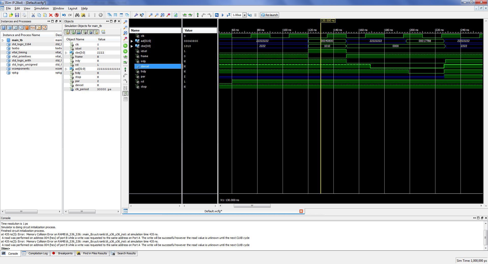
As described above, the device uses type 0 transactions for processing by the device. Since the device is one-function, the function number is 000, which are checked in the control machine. Depending on the register number (bits 7..0 of the AD bus), the required register is sent to the AD bus, as shown in the figure above.
Configuration read code
signal CfgRData: std_logic_vector(31 downto 0):=x"00000000"; signal CommandReg: std_logic_vector(15 downto 0) := x"0000"; signal StatusReg: std_logic_vector(15 downto 0) := x"0200"; signal LatencyTimer: std_logic_vector(7 downto 0) := x"00"; signal CacheLineSize: std_logic_vector(7 downto 0) := x"00"; signal BAR0: std_logic_vector(31 downto 0) := x"00000001"; signal BAR1: std_logic_vector(31 downto 0) := x"00000000"; signal InterruptLine: std_logic_vector(7 downto 0); process (clk_I) begin if (rising_edge(clk_I)) then case (Address(7 downto 0)) is when x"00" => CfgRData <= x"00017788" ; --Device ID and Vendor ID when x"04" => CfgRData <= StatusReg & CommandReg; --Status Register, Command Register when x"08" => CfgRData <= x"10000001"; -- Class Code and Revision ID when x"0C" => CfgRData <= x"0000" & LatencyTimer & CacheLineSize; -- BIST, Header Type(bit 7 = 0, single, bits 6-0 = 0, type0), Latency Timer(for masters), Cache Line Size (bit 2 in 1) when x"10" => CfgRData <= BAR0; -- Base Adress 0 (Register IO address decoder) when x"14" => CfgRData <= BAR1; -- Base Adress 1 when x"28" => CfgRData <= x"00000000"; -- CarfdBus CIS Pointer when x"2C" => CfgRData <= x"00017788"; -- Subsystem ID, Subsystem Vendor ID when x"30" => CfgRData <= x"00000000"; -- Expanxion Rom Base Address when x"34" => CfgRData <= x"00000000"; -- Reserved, Capabilitis Pointer when x"38" => CfgRData <= x"00000000"; -- Reserved when x"3C" => CfgRData <= x"004001" & InterruptLine; -- Max_Lat(only bus master), Min_Gnt, Interrupt Pin, Interrupt Line when others => CfgRData <= (others => '0'); end case; end if; end process; This is how the configuration reads in the simulator:

Configuration record
On the AD bus, the master sets the address of the register to be written, and in the next cycle, the data to be recorded is set. In BAR0, bits 7..0 are read-only, in BAR1, bits 15..0 are read-only. Therefore, 256 I / O addresses, 4 294 967 296 memory addresses.
Configuration Write Code
process(clk_I, RST_I) begin if(RST_I = '0')then CommandReg <= x"0000" after cTCQ; StatusReg <= x"0200" after cTCQ; LatencyTimer <= x"00" after cTCQ; CacheLineSize <= x"00" after cTCQ; BAR0 <= x"00000001" after cTCQ; BAR1 <= x"00000000" after cTCQ; elsif(rising_edge(clk_I)) then if (smPCI_T = sCFG_WRITE) then case(Address(7 downto 0)) is when x"04" => if (CBE_I(1) = '0') then CommandReg(15 downto 8) <= AD_I(15 downto 8) after cTCQ; end if; if (CBE_I(0) = '0') then CommandReg(7 downto 0) <= AD_I(7 downto 0) after cTCQ; end if; when x"0C" => if (CBE_I(1) = '0') then LatencyTimer <= AD_I(15 downto 8) after cTCQ; end if; if (CBE_I(0) = '0') then CacheLineSize <= AD_I(7 downto 0) after cTCQ; end if; when x"10" => if (CBE_I(3) = '0') then BAR0(31 downto 24) <= AD_I(31 downto 24) after cTCQ; end if; if (CBE_I(2) = '0') then BAR0(23 downto 16) <= AD_I(23 downto 16) after cTCQ; end if; if (CBE_I(1) = '0') then BAR0(15 downto 8) <= AD_I(15 downto 8) after cTCQ; end if; when x"14" => if (CBE_I(3) = '0') then BAR1(31 downto 24) <= AD_I(31 downto 24) after cTCQ; end if; if (CBE_I(2) = '0') then BAR1(23 downto 16) <= AD_I(23 downto 16) after cTCQ; end if; when x"3C" => if (CBE_I(0) = '0') then InterruptLine <= AD_I(7 downto 0) after cTCQ; end if; when others => null; end case; end if; end if; end process; Port Record
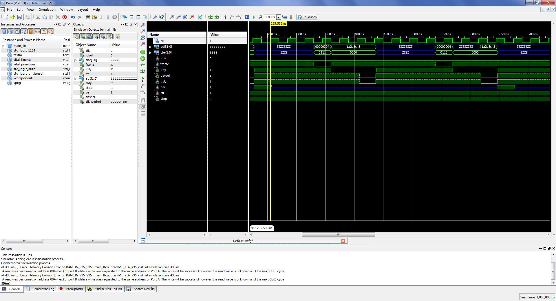
On the AD bus, the master sets the register number for recording; in the next cycle, the data to be recorded is set.
We give an example for recording only one register, the rest are written in a similar way.
signal IOReg0: std_logic_vector (31 downto 0); process(clk_I, RST_I) begin if(RST_I = '0') then IOReg0 <= x"00000000" after cTCQ; elsif (rising_edge(clk_I)) then if (smPCI_T = sIO_WRITE and Address(7 downto 0) = x"00") then if (CBE_I(0) = '0') then IOReg0( 7 downto 0) <= AD_I( 7 downto 0) after cTCQ; end if; if (CBE_I(1) = '0') then IOReg0(15 downto 8) <= AD_I(15 downto 8) after cTCQ; end if; if (CBE_I(2) = '0') then IOReg0(23 downto 16) <= AD_I(23 downto 16) after cTCQ; end if; if (CBE_I(3) = '0') then IOReg0(31 downto 24) <= AD_I(31 downto 24) after cTCQ; end if; end if; end if; end process; Port reading
On the AD bus, the master sets the register number to be read. The device then sends the requested data to the AD bus.
Read port code
signal IORDate: std_logic_vector (31 downto 0); process (clk_I, RST_I) begin if (RST_I = '0') then IORDate <= x"00000000"; elsif (rising_edge(clk_I)) then case (Address(7 downto 0)) is when x"00" => IORDate <= IOReg0 after cTCQ; when x"04" => IORDate <= IOReg1 after cTCQ; when x"08" => IORDate <= IOReg2 after cTCQ; when x"0C" => IORDate <= IOReg3 after cTCQ; when x"10" => IORDate <= IOReg4 after cTCQ; when x"14" => IORDate <= IOReg5 after cTCQ; when x"18" => IORDate <= IOReg6 after cTCQ; when x"1C" => IORDate <= IOReg7 after cTCQ; when x"20" => IORDate <= IOReg8 after cTCQ; when x"24" => IORDate <= IOReg9 after cTCQ; when others => IORDate <= (others => '0'); end case; end if; end process; This is what the I / O port reads and writes:

Write and read memory
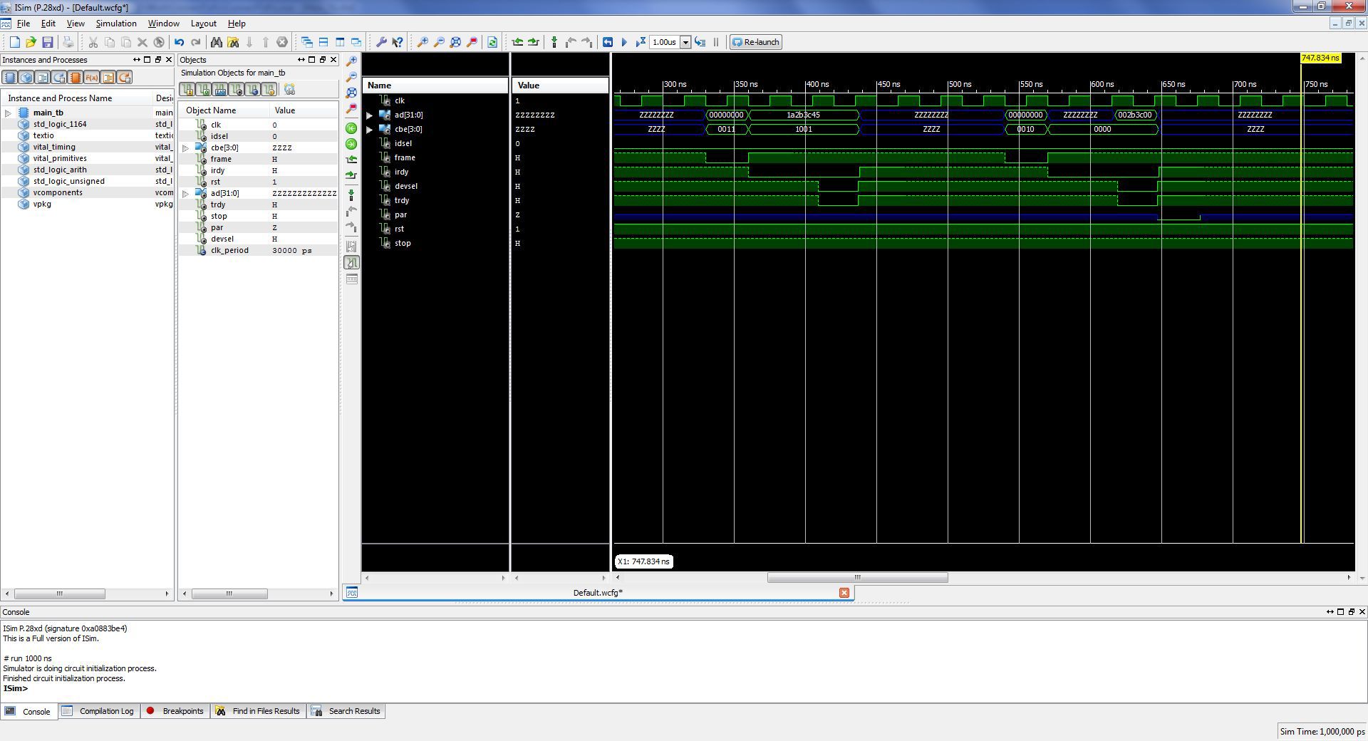
On the AD bus, the master sets the address to which the data is to be written, and in the next cycle the data itself. When reading on the AD bus, the master sets the address for reading, then the target itself sets the data on the AD bus.
Data is written in RAM to port A, read from port B.
Memory access code
signal RamWrEn: std_logic; signal RamOutputDate: std_logic_vector (31 downto 0); signal RamInputDate: std_logic_vector (31 downto 0); signal RamRst: std_logic := '0'; RAMB16_S36_S36_inst : RAMB16_S36_S36 port map ( DOA => open, -- Port A 32-bit Data Output DOB => RamOutputDate, -- Port B 32-bit Data Output DOPA => open, -- Port A 4-bit Parity Output DOPB => open, -- Port B 4-bit Parity Output ADDRA => Address(8 downto 0), -- Port A 9-bit Address Input ADDRB => Address(8 downto 0), -- Port B 9-bit Address Input CLKA => clk_I, -- Port A Clock CLKB => clk_I, -- Port B Clock DIA => RamInputDate, -- Port A 32-bit Data Input DIB => x"00000000", -- Port B 32-bit Data Input DIPA => x"0", -- Port A 4-bit parity Input DIPB => x"0", -- Port-B 4-bit parity Input ENA => '1', -- Port A RAM Enable Input ENB => '1', -- PortB RAM Enable Input SSRA => '0', -- Port A Synchronous Set/Reset Input SSRB => '0', -- Port B Synchronous Set/Reset Input WEA => RamWrEn, -- Port A Write Enable Input WEB => '0' -- Port B Write Enable Input ); process(clk_I) begin if (rising_edge(clk_I)) then if (RST_I = '1') then RamRst <= '0'; else RamRst <= '1'; end if; end if; end process; process(clk_I, RST_I) begin if(RST_I = '0') then RamInputDate <= (others => '0') after cTCQ; RamWrEn <= '0' after cTCQ; elsif (rising_edge(clk_I)) then if (smPCI_T = sMEM_WRITE) then if (CBE_I(0) = '0') then RamInputDate(7 downto 0) <= AD_I( 7 downto 0) after cTCQ; end if; if (CBE_I(1) = '0') then RamInputDate(15 downto 8) <= AD_I(15 downto 8) after cTCQ; end if; if (CBE_I(2) = '0') then RamInputDate(23 downto 16) <= AD_I(23 downto 16) after cTCQ; end if; if (CBE_I(3) = '0') then RamInputDate(31 downto 24) <= AD_I(31 downto 24) after cTCQ; end if; RamWrEn <= '1' after cTCQ; else RamWrEn <= '0' after cTCQ; end if; end if; end process; It looks like the recording and reading of memory in the simulator:

Data on the AD bus is displayed as follows. Depending on the state of the machine, the corresponding register is connected to the output buffer.
process (clk_I, RST_I) begin if (RST_I = '0') then AD_O <= (others => '0') after cTCQ; elsif (rising_edge(clk_I)) then if (smPCI_T = sCFG_READ) then AD_O <= CfgRData after cTCQ; elsif (smPCI_T = sIO_READ) then AD_O <= IORDate after cTCQ; elsif (smPCI_T = sMEM_READ) then AD_O <= RamOutputDate after cTCQ; end if; end if; end process; The data enable signal to the AD bus is formed as follows:
process (clk_I, RST_I) begin if (RST_I = '0') then AD_T <= '1' after cTCQ; elsif (rising_edge(clk_I)) then AD_T <= not b2l(smPCI_T = sCFG_READ or smPCI_T = sIO_READ or smPCI_T = sMEM_READ) after cTCQ; end if; end process; Separately, I would like to add about the component STS for example signal generation DEVSEL
DEVSEL_STS : entity WORK.componentIO(Behavioral) port map (iD => DEVSEL_O, oT => DEVSEL_T, clk => clk_I, rst => RST_I) Since the active levels of control signals are equal to zero, in order to go to Z - state and release the line you need to first give the level of a logical unit and then transfer to the Z - state.
Conclusion
In conclusion, I want to say that the execution of transactions on the PCI bus is not as difficult as it seems. Designed firmware was embedded in FPGA. The board with FPGA is inserted into the PCI slot and the computer was turned on. The system found a board and requested drivers for it.


Works! :)
The project itself is drive.google.com/file/d/0B-i4aT8Q0ZNxc1VkV3J2b0dTRlU/view?usp=sharing . Open xilinx ise 14.2.
Source: https://habr.com/ru/post/182152/
All Articles