Graphene photosensor is 1000 times more sensitive to light than CMOS and CCD
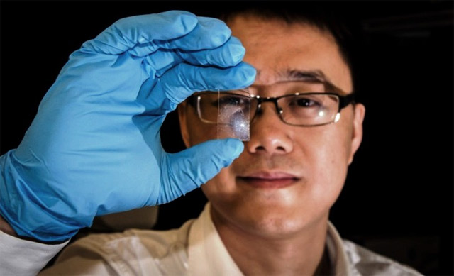
A group of scientists led by associate professor Wang Qijie from Nanyang Technological University (Singapore) announced the development of a graphene-based photo detector . In all respects, it is superior to current CMOS and CCD sensors, approximately 1000 times more sensitive to light than the previously created experimental graphene photodetectors, consumes 10 times less energy and 5 times cheaper than modern CMOS matrices.
Graphene is a carbon film one atom thick. One square meter of material weighs only 0.77 milligrams. The material differs in that it has a forbidden energy zone equal to zero, thanks to which it can absorb photons of any energy. Moreover, graphene, when absorbed by a single photon, transforms it into several electrons at once. These qualities of the material and allows you to make on its basis a high-sensitivity photo detector.
The sensor using the graphene layer is "1000 times more sensitive to light than cheap sensors from modern compact cameras," according to a press release on the university website. Moreover, the graphene sensor consumes an order of magnitude less energy, since it requires less electrical voltage.
')
In the end, new-type sensors will be about five times cheaper than modern CMOS sensors. For their production, it is not necessary to drastically change the technical process, because they were originally created for manufacturing on the current conveyors for stamping CMOS matrices. Only a small modernization of the technical process in connection with the replacement of the base material in the photosensitive layer will be required.
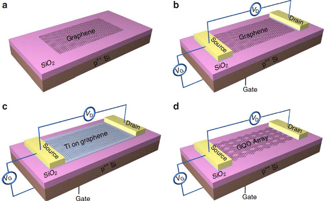
The device manufacturing process: (a) a single graphene layer is mechanically layered on a 285-nanometer SiO 2 / Si substrate; (b) a field-effect transistor is made of a graphene photodetector: a source and a Ti / Au drain (20 nm / 80 nm) made by photolithography are added, and a gate is made on the back side of the substrate; (c) a nanometer “sacrificial” layer of titanium is deposited on the surface of graphene by the method of electron beam evaporation; (d) The “sacrificial” titanium layer is removed by wet etching, after which a grating with quantum dots of various sizes can be formed on a silicon substrate, depending on the thickness of the titanium layer.
The graphene nano-lattice detects photons for the entire spectrum of visible light, as well as for infrared radiation of the near and middle ranges. Thus, the new sensors are suitable not only for conventional digital cameras, but also for outdoor surveillance cameras, infrared cameras, road cameras, satellite photography, etc.
Increasing the photosensitivity a thousand times will completely eliminate the use of flash units. Even moonlight should be enough to get a high-quality saturated image. It is possible that the sensor will be able to register the glow of bodies, the radiation of which was previously not recorded at all by instruments.
The scientific work "Broadband high photoresponse from pure monolayer graphene photodetector" was published in the journal Nature Communications.
Source: https://habr.com/ru/post/181864/
All Articles