A quick look at DesignSpark PCB
 Traditionally, when designing printed circuit boards for electronics of varying degrees of DIY, most people use almost the same set of software: Proteus, EagleCAD, SprintLayout, etc. Until recently, Proteus + SprintLayout met all my needs, however, Proteus had to succeed, but I didn’t have a good relationship with other CAD-based e-targeting programs (out of those that were “heard”) window did not want to.
The search for alternatives led me to the site of the bourgeois DesignSpark PCB program, and continued use prompted me to write this short review.
From my purely subjective point of view, the ease of use of such CAD programs is 80% of two points:
- Convenience to create your own electronic components
- Convenience of tracing boards
These two points will be discussed further.
Disclaimer
All the drawings described in this article are created exclusively for this article. They do not claim for optimality, elaboration, compliance with any norms and standards. They have never been and will not be created by the author, so even the performance of the boards is not confirmed by anything. Any assessments, comparisons, comparisons and conclusions are 100% subjective.
A few words about the program itself
The first and probably the most pleasant impression is the shareware program. And in this case, the concept of conditional gratuity is disclosed in a favorable manner and differs markedly from the concept of temporary gratuity or gratuity with limited functionality. After installation, an activation code is requested, an activation code is issued on the site after registration - everything is simple. After indicating the profile of the “engineer” profession, I received a license for 6 computers. Another useful side of registration is the presence on the site of an open database of electronic components. The base is huge, but filled with very fragmented.
')
The second is that the program belongs to the class of “full cycle programs”, as I call it, i.e. on the basis of the concept (one or several), a board is created and divorced, along with all the checks are performed and you can immediately mutate the 3D model of the future scarf.
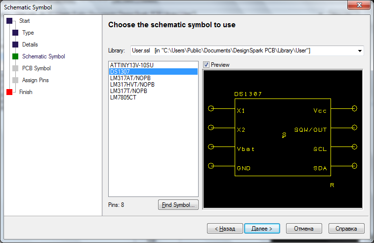
DS1307
The easiest way to describe the process of creating a component for a user library is an example of some kind of microcircuit; in this case, the DS1307 in the DIP-8 package will become the experimental one.
The process itself is similar to that in the Eagle CAD environment:
- Draw schematics
- Draw a body (one or more)
- Blind the schematics and corpuses together by matching the schematic conclusions with the real ones.
Take a look at the structure of the library catalog:
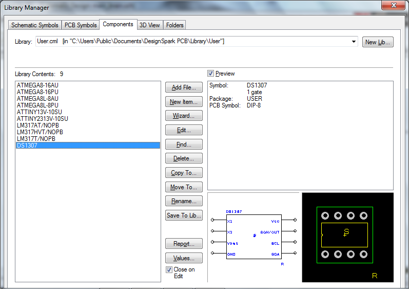
Library catalog. Schematic separately, shells separately, the components created from them are also separate.
In the screenshot above, what I got as a result.
The designer is responsible for the process of drawing electronic components - a separate designer for each design stage of our future parts: Symbol Wizard, Footprint Wizard, Component Wizard. Now about each detail.
Symbol Wizard
Launch Symbol Wizard, which offers to draw a schematics.

The main stages of component rendering are described on the left.
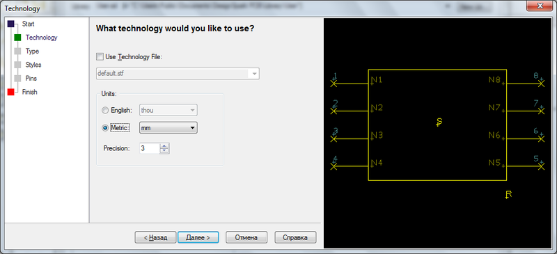
The technology can be left “by default”. We select the metric measurement system for the sake of convenience and follow below.

Select the type / type of the symbol of the future parts and positioning of the labels relative to the scheme.
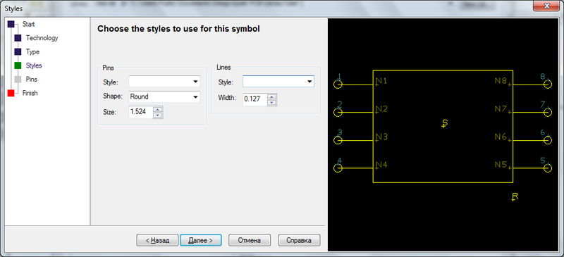
Set pin display styles and their sizes.
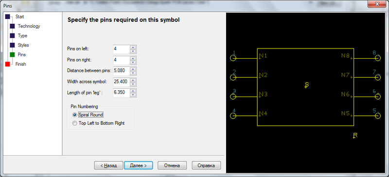
Finally, we set the number of pins on the left and right, the distance between them, their length, and the order of numbering.
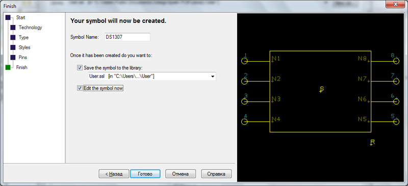
We assign the name to the created symbol and save it to the user library of symbols. By the way, in this case I used the name of the created chip, although it would be more reasonable to call the component as “PIN-8”, since the once created schematics can be later used for any other component with the appropriate number of legs.

That's what happened in the end. The inscriptions N1-N9 at the stage of creating a component based on this schematics will be replaced with their corresponding names. In this screenshot for clarity, I signed their resulting values.
Footprint wizard
Footprint Wizard is responsible for the creation of PCB-models of electronic components exactly like the Symbol Wizard. The same designer, only we create now the case.
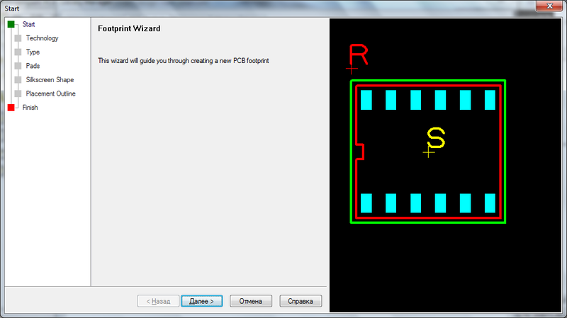
The process is almost completely identical and kills its simplicity in comparison with the same Eagle CAD.
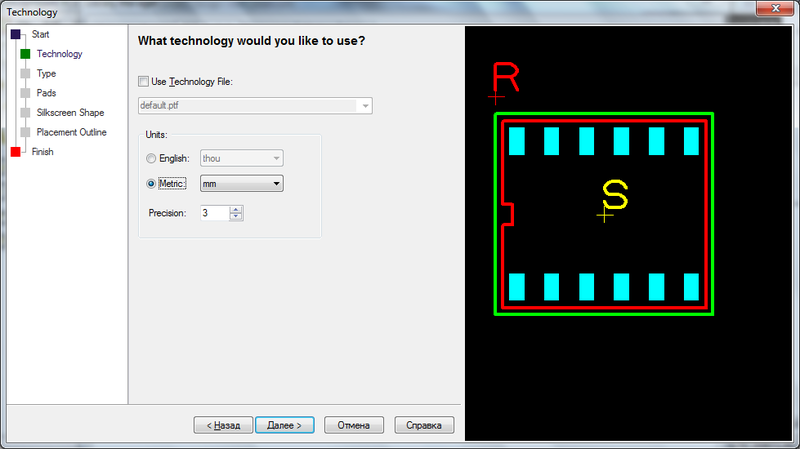
We leave the technology “by default”, set the metric system.

Select the type of case and the positioning of the inscriptions (this is for silk-screen printing).
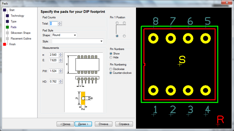
We set the parameters of the pads under the legs: their number, size, style, distance between the legs and the order of numbering.
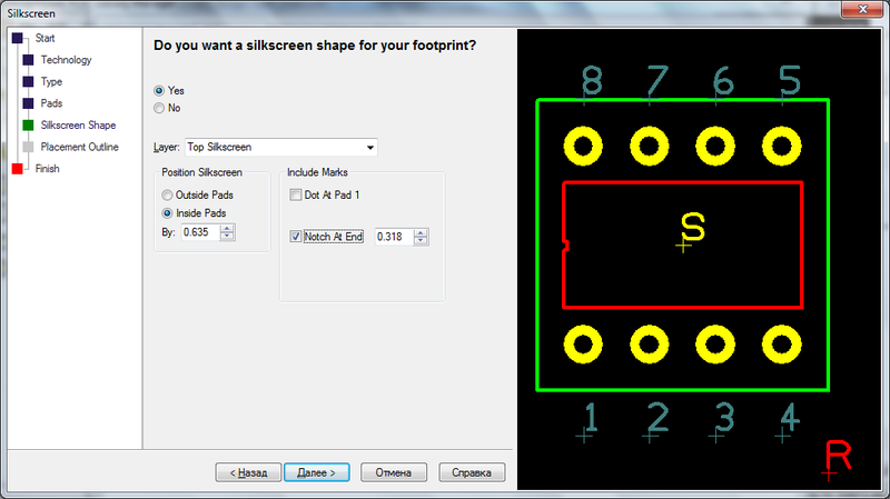
Set a model for screen printing. I have a rectangle inside the pads, although it usually happens the other way around - outside, but I like it better.

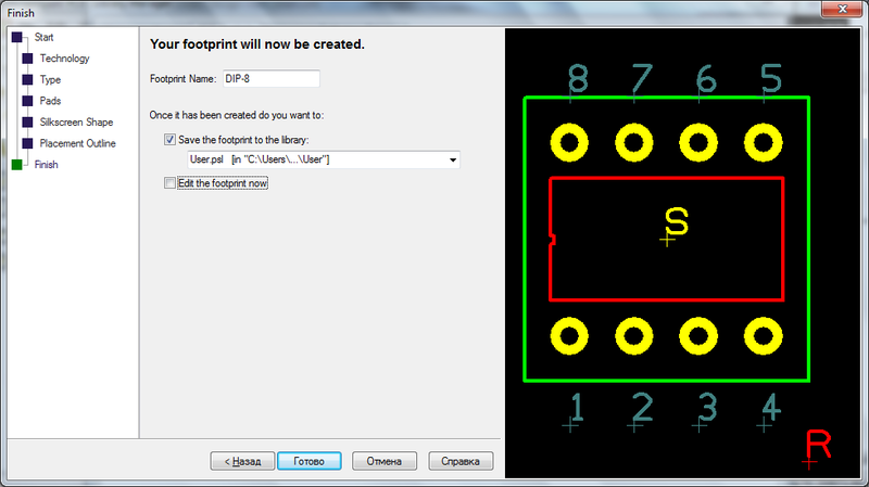
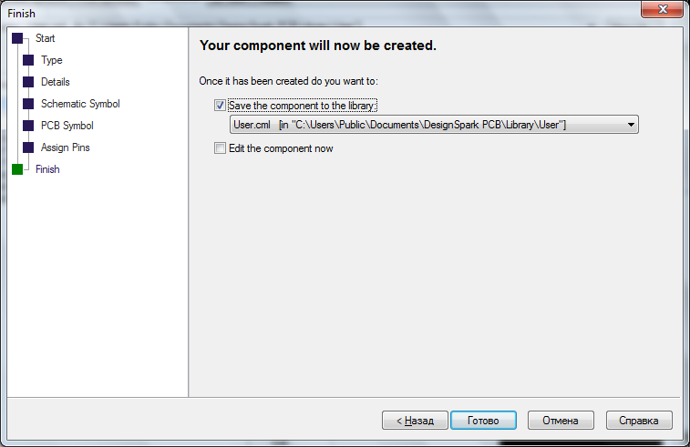
The last but one step is to choose whether or not to indicate the external borders indicated for the component, after which you can either simply save the resulting PCB model or go straight to manual editing of the result, which depends on the state of the Edit the footprint now checkbox at the time you click the Finish button.
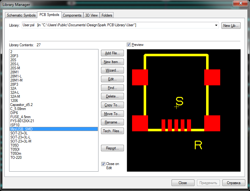
In the manual editing mode, you can delete anything or draw to the model created in the constructor. For example, a mini-USB model for SMD mounting is obtained from half of the contacts from the SOIC-10 case and four square pads.
Creating an electronic component from schematic and PCB models is, in fact, a simple comparison of schematic pins with pads of a PCB model. There is also a constructor for this, but since it is identical to the ones presented above, I will hide it.
Screenshots of the Component Wizard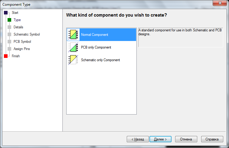


Board trace
... starts in 2 clicks. :)
The tracing scheme looks like this:

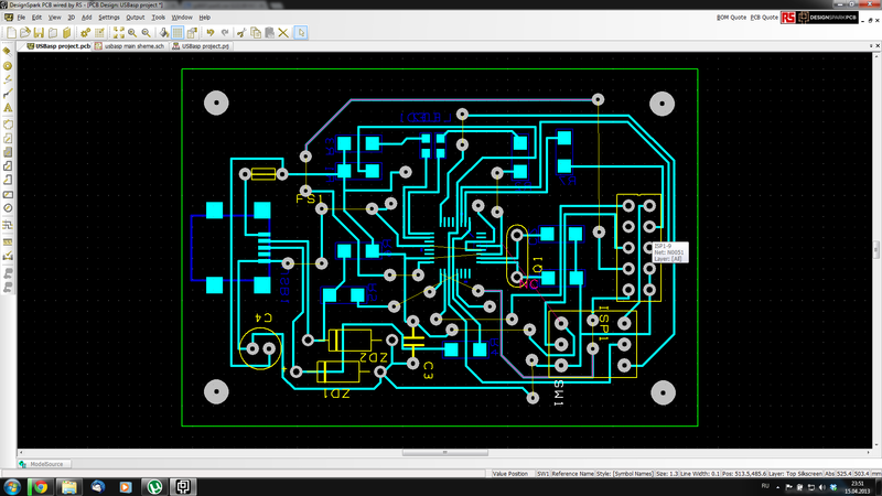
Slightly modified USBasp programmer
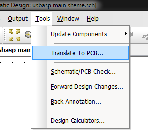
Without departing from the traditions of this program, 2 clicks on Tools - Translate to PCB ... will launch the next designer - the designer of the future board.
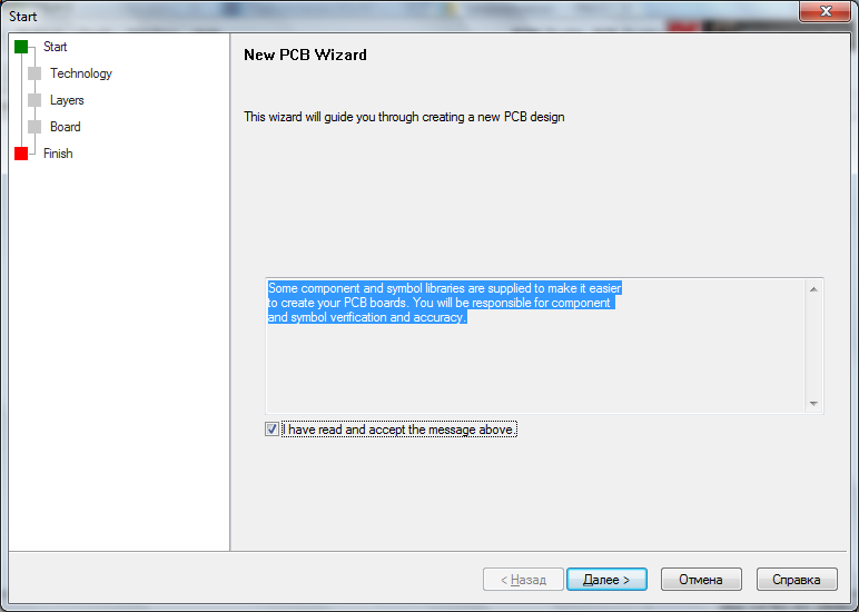
We read (or do not read) the message, agree or refuse to create a fee - at your discretion.
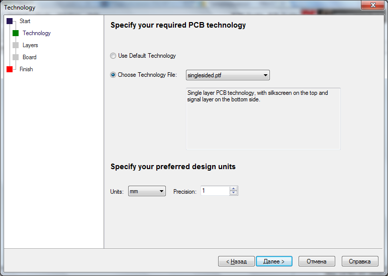
I will speak about the notorious technology files later in the text, now you can leave the default technology and mm as units of measurement (or thou, if it is more convenient for someone).
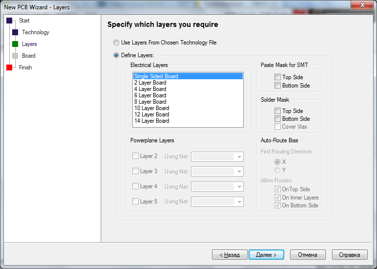
This screenshot clearly shows why the technology in the previous paragraph, you can leave the default. Select the number of layers (from 1 to 14) and indicate on which layers to place the soldering mask.
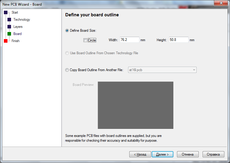
Specify the starting dimensions of the board or diameter, if the board is round. "Starting" dimensions only because then all the same, all these parameters are easily changed.
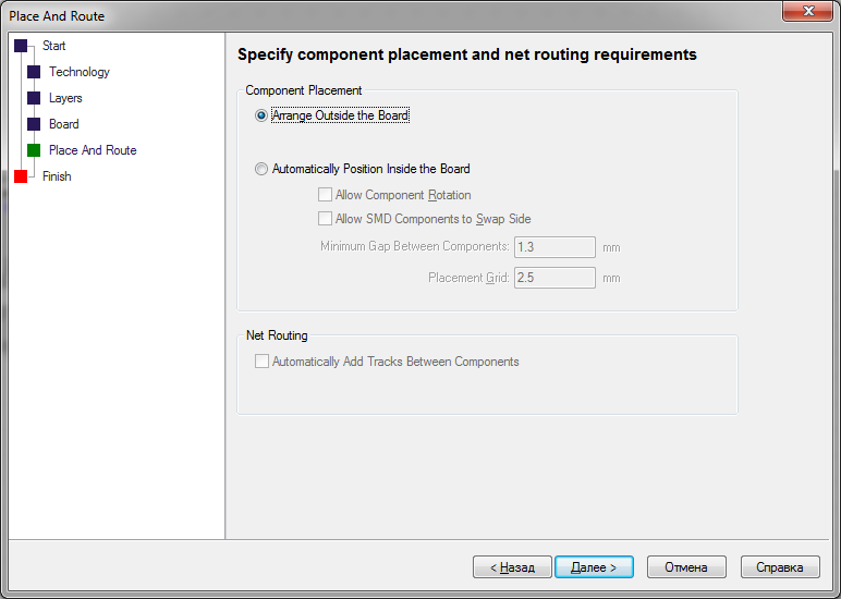
"Placement and tracing." There is no point in automatically placing the components on the board and tracing the tracks between them - the heap will be small with a long list of undivided tracks. There is an autotracer, but it spreads badly.
The result of all these actions will be a picture similar to the one below:

Silhouette boards, components, communications. Just like in Eagle CAD.
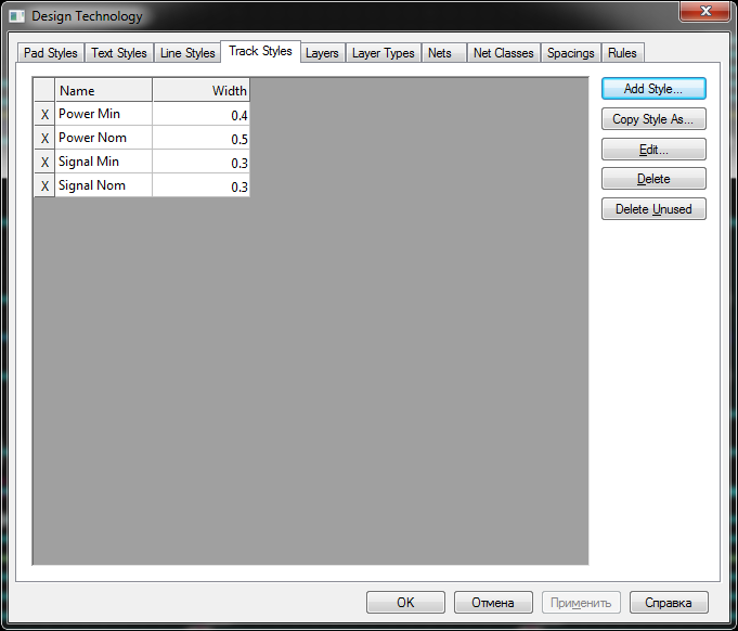
However, before placing components on the board and making tracks, you need to say a few words about the technology file that was left default in the constructor. This file controls the technological standards used for wiring: the width of the power and signal tracks, the distance between them, between the tracks and components, etc. And right now, before starting the trace, it is best to take care of it. Its settings are located in Settings - Design Technology, externally they look like a table into which the required values fit.
Then you can already place the components, build tracks, run checks, correct errors, etc.
There are several checks, I will mention only the main one - Design Rule Check . It checks the observance of all the rules that are described in the technological files: distances, connections, gaps, intersections, etc.
The report on checks in the * .txt format will appear in the project folder.
In conclusion, a few words about the possibilities of export.
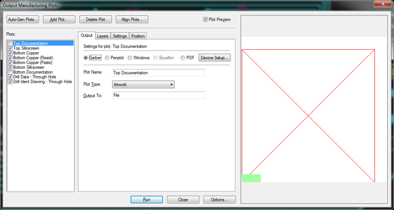
In addition to the most popular format Gerber, there is the possibility of exporting to DXF, which, in fact, is a universal exchange format for drawings. From here and the corresponding possibilities of the subsequent import into AutoCAD or any other program supporting DXF, of which there are now quite a lot.
You can download the program from the official site .
Source: https://habr.com/ru/post/181634/
All Articles