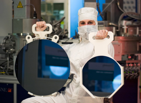
Features of the transition from 300 mm to 450 mm silicon wafers
Some readers probably know that the transition to the new standard promises a considerable reduction in the cost of chips. With such an advantage of using larger plates, the reasons for delaying the transition to a new standard do not seem obvious. It may even seem that all this is nothing more than a global conspiracy of corporations seeking to halt progress in order to obtain super-profits, whereas all that is needed is to buy new machines. "It's so easy!" - thinks a man in the street.
I propose to remove the foil cap and understand the problems that arise when scaling, and the technical details of the production of silicon wafers. This article lists only a few.
')
Investment and payback
For a start, let's figure out why all this bother with the increase in the size of the plates? The fact is that as the plate increases, the cost of each chip drops. Calculations show that the transition from the current 300 mm to 450 mm will eventually save about 30%. Approximately the same as happened when moving from 200 to 300 mm plate.
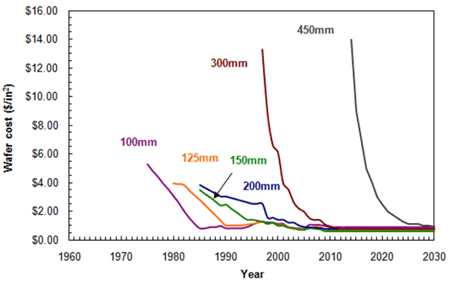
Reducing the cost of chip production by 30% is really significant. But with a note that this will happen far from immediately, since initially the cost of new plates will be much higher. The cost of square. cm 450 mm of the substrate is equal to the current price square. cm 300 mm of the substrate is not earlier than 2025. And at the beginning of use it will be 4-5 times more expensive.
General transition trends are as follows:
- 30-100% increase in value
production areas, those. maintenance and equipment for
automation. - 20-50% increase in value
lithographic equipment. - 10-30% reduction in throughput
projection equipment capabilities. For the rest of the equipment
- without changes. - 15% reduction in labor costs.
- 70% increase in reagent costs.
Estimated investment costs can go as high as $ 60 billion, and therefore the largest producers, willy-nilly, have to combine their efforts to move to a new standard. The payback of such a large investment is about 8 years. At least the R & D of the transition from 200 mm to 300 mm plates paid off approximately in such a period.
Well, where is the savings? The answer is not so simple.
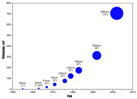
The area of the silicon substrate increases by as much as 2.25 times. In addition, even more chips can be placed, since the rectangles fit into a circle with a large radius with greater efficiency. Speaking in a simple way, if you draw a circle with squares, the circle will be “rounder” than it is larger or smaller squares.
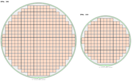
Take for example the Tahiti XT core with an area of 352 mm2, which is the basis of HD 7970 graphics cards. Provided that the chips are square, about 160 chips can be placed on a 300 mm substrate, and 386 on 450 mm substrate (see the figure below). That is 2.41 times more. Of course, the increase will vary depending on the size of the chip.
It follows from this that a factory with a production capacity of 40–45 thousand plates is capable of producing as many chips as the 300 mm factory with a capacity of 100 thousand plates. And just this moment allows you to save! A 450 mm factory for 40 thousand plates will cost 25% less than a 300 mm factory for 100 thousand plates. Savings are largely due to lithographic equipment, the cost of which does not increase commensurately as power, as noted above.
But there is a nuance. With other listed factors increasing the cost of production, the current cost of lithographic equipment would not compensate for the costs if it remained unchanged. Fortunately, the cost of equipment for every more advanced tech. the process grows, and with it the benefit of switching to a larger plate diameter.
Technical difficulties
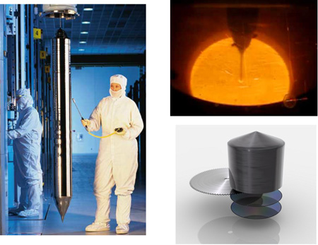
Crystal weight
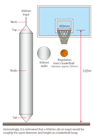
The weight of the grown crystal increases by 3 times, to one ton. There is a problem with the vertical suspension of the crystal by a narrow neck, a few mm thick, during the growing process. The seed crystal alone will not be able to withstand the weight of 450 mm of the crystal. Need an additional way to maintain the crystal.
Growing time
Any external vibration (for example, an earthquake) can cause a change in the spatial lattice of the crystal. If this happens, the crystal has to be completely melted and the growth begins from the very beginning. This takes a significant amount of time (up to a month) and thus increases the cost of production.
Since the effects of the earthquake in Japan in 2011 reduced the global production of silicon single crystals by 24.5%. In fact, grown crystals turned into garbage. It took more than a month to restart production.
Quartz crucibles
Quartz crucibles for melting polycrystalline silicon should be larger and must withstand twice the time required for production than 300 mm crystals used to grow.
If for growing 300 mm of crystals, crucibles with a size of 81.3 cm are used, then for 450 mm of crystals, crucibles with a diameter of up to 111 cm are needed. To withstand such a long time of cultivation, the quality of crucibles must also be improved.
Cooling
The cooling time may increase up to 4 times.
The thermal past, during crystal production, affects the amount, size and distribution of defects as impurities. Unlike offsets, such defects are usually present. And although they do not necessarily lead to the rejection of the crystal, but it can affect the performance of the final chips. Therefore, you need to accurately control the process to minimize their appearance. Due to the enormous size of the 450 mm crystal, it will cool more slowly, which exposes it to a higher temperature difference and affects the appearance of defects. This requires an innovative cooling process.
Conclusion
Summing up, the transition to the 450 mm plate is the need to compensate for the ever increasing cost of lithographic equipment. Getting on this train is very expensive, but not to sit down at all is to put yourself at a disadvantage relative to competitors in the long run. In addition, it is important to know the optimal time for landing.
So manufacturers can be easily understood, especially considering the possible risks that may arise over such a long period of time. It can be everything, starting with global economic problems, ending with the fact that more promising technologies may appear even before the investment pays off.
Yes, by the way, if you have not yet understood, for us, consumers, the transition will not be reflected in the reduction in the cost of processors, GPU and memory. At least not in this decade.
Sources:
www.sumcosi.com/english/products/next_generation/problem.html
A Simulation Study of 450mm Wafer Fabrication Costs
Economic Analysis of 450mm Wafer Migration
Reaping the Benefits of the 450mm Transition
Indistinguishable From Magic: Manufacturing Modern Computer Chips
www.silicon-edge.co.uk/j/index.php?option=com_content&view=article&id=68
Source: https://habr.com/ru/post/177073/
All Articles