3D integration: what are the difficulties?
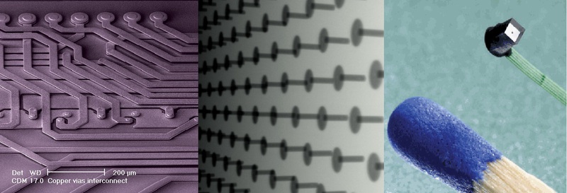
KDPV on the right - a miniature camera (62.5 thousand pixels), made possible by connecting to an optical sensor via TSV
In one of the previous posts , I talked about what 3D integration is and how this technology could extend the life of silicon electronics by growing into a third dimension. This time I will try to describe the problems of this technology known to me, because of which now and in the next few years “multi-storey” microprocessors and the memory of a new generation will not appear in stores. It is always easier to argue with arguments than to praise :). So…
To begin with - about making holes in the silicon wafer. The thickness of silicon wafers used for lithography varies from ~ 20 to ~ 800 microns. In this case, the lower layer is usually in the category> 250 μm, and the rest in the category <60 μm. There are several reasons for this, including mechanical strength. So, there is an acute problem of how to make a lot of neat holes in a layer of silicon, even 20 microns thick, and without damaging the plate itself (transistors are already on it or will be three orders of magnitude smaller). There are several technologies for making holes and traditionally there is a choice between accuracy and speed, which means price. I will give a few images.

The hole obtained using laser pulses (40ns, 100KHz) (9400 pcs./19 min.)
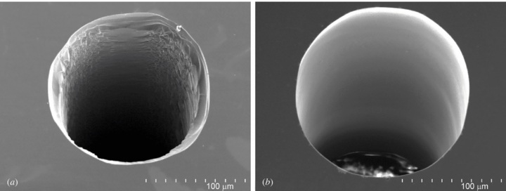
Results of chemical etching of laser-cut holes (20min./plate)
')
The next step is to metallize the holes . Here, too, there are a number of their problems.
The first is the size of TSV, and transistors differ by 2-3 orders of magnitude, therefore, if you try to transfer such amount of metal into the hole in the same way, it will be a long time. Rather, LONG, and expensive.
Secondly, due to the fact that the metal should be applied not on a flat surface, but on the inner walls of the hole, the holes tend to “overgrow”. That is, the metal completely closes the inlet, and without fully covering its walls and without creating a through conductive bond. Additional efforts should be made to solve this problem.
There are interesting approaches, like “driving” into the holes of a metal pin, with obvious problems, both from the discharge of precision operations and the safety of the plate.
Next are the problems of assembling a stack of silicon wafers using TSV (vertical joints). 3d integration is primarily important for large devices, since could greatly reduce their cost by reducing the area of the silicon wafer rejected by a single defect. But instead, the problem is modified: now, when laying one plate on another, it is required to connect hundreds and thousands of TSV contacts with each other. And to do it from the first time, there will be no second attempt. Such exercises with TSV sizes of the order of units or tens of microns lie in the field of exact mechanics, which has its limitations. And the price of a mistake is the failure of the whole stack of plates. That does not affect the price positively.
At the same time, around TSV, when developing, it is necessary to leave some “exclusion zone” free of transistors. Otherwise, the risk is too high that, in the process of cutting holes or assembling a stack of plates, the logic in this area will be damaged. On the one hand, this increases the occupied space, and on the other hand, it requires taking such things into account during the design process.
The mechanical strength of such a product is a separate problem. The presence of through holes in itself reduces the strength of the plates. In addition, for reasons of load distribution, it would be better to position the holes evenly. Also, such a “sandwich” of silicon wafers will have non-uniform characteristics of thermal expansion. When the operating temperature drops, this creates a significant force at the TSV junction points and can lead to destruction of the stack.
But the main problem, of course, is maintaining the temperature . In order to ensure the temperature below 80 degrees, you have to go for various tricks. For example, experts from IBM suggest alternating silicon wafers with wafers with high thermal conductivity, creating a kind of "penetrating radiator" that removes heat more efficiently than just contacting the surface.
In theory, there are no restrictions on how many plates can be combined using 3d integration. But, even for memory, where the problem with heat generation is not so acute, plans for the future are limited to eight layers.
The temperature regime is also the reason why the 3d-integration technology was outside Intel's interests, despite the fact that a number of other companies in the industry were actively developing and trying to use it. Until relatively recently, the mobile device market was not a priority, and all efforts were aimed at creating desktop and server processors. In this case, the main goal was to increase productivity, and not to reduce energy consumption. The greatest benefit could be obtained by applying 3d integration to large chips, such as Itanium. But temperature problems actively interfere with this.
An interesting problem in some cases may be testing and debugging of such devices. Imagine the separation into plates not as “processor separately, memory separately”, but something more interesting, where each plate is not a complete device and does not work separately from the others. In such a situation, the question arises, how to check the functioning of each plate before stacking? If we refuse such a check, then the probability that the end device will not work due to the plate connection errors will add the probability that one of the plates will not function.
And finally, in order, and not in importance. Development of devices using 3d integration requires appropriate support by means of design automation . A number of companies have been concerned about this for a long time, in particular, Synopsys has been working in this direction, at least since 2009. But it is a long process. Efforts are not limited to man-hours of developers, and much remains to be done.
On this I will finish. A huge number of more specific problems is hardly of interest to the general public. Yes, and what has been written above should be enough to understand that 3d integration is not a “silver bullet” and there are many problems on the way to it.
Perhaps there will be another post dedicated to a number of exotic applications of 3d-integration technology.
Source: https://habr.com/ru/post/173347/
All Articles