Other side 22nm: unknown heroes of Silicon Valley
Every few years, Intel announces a transition to a new technological process. If we add news from other semiconductor companies here, then the year does not pass, so that one or another of them does not announce a new breakthrough. The names of these companies are well known and widely known. But in their shadow (completely undeserved) one company was lost, whose work invisibly stands almost behind each of the technological advances in semiconductor technology. “A country must know its heroes” ...
It's about a little-known company Applied Materials, which has simply been doing its job for over 45 years. And today, at every factory producing silicon chips from Intel, TSMC, Global Foundries, and almost any other equipment installed Applied Materials, which performs almost the smallest work known to mankind. At the same time, the matter is not limited to the production of microcircuits, Applied Materials also had a hand in the production of liquid crystal screens and solar batteries. If a company deals with silicon wafers, it can be stated with almost 100% probability that Applied Materials equipment is responsible for most of the manufacturing process.

Company logo, who ever saw him before?
In particular, when Intel announced the transition to 22nm technology, it achieved this using Applied Materials equipment. This does not make Intel's achievement less outstanding: Applied Materials provides the hardware, but everything else lies on Intel from the design of microprocessors to the search for suitable chemical compounds. It is also important to note that AMD, Samsung and TSMC essentially have access to the same hardware as Intel.
What is it about microprocessor manufacturing?
Many have heard of the lithography process. But if you think that the manufacture of a processor crystal only consists of it, then you are mistaken. Yes, lithography is a vital part of the process, but for modern technical processes 45nm and 32nm, not to mention 22nm Fin-FET, this is only one of hundreds of steps. After the silicon surface has been subjected to lithography, transistors and their connections are grown on it, using a combination of galvanic processes, ion implantation, chemical deposition, molecular layering, and many others. In addition, most of these operations can be divided into tens of steps.
')
On the Internet there are many videos that show the production of microprocessors (for example: this ).
All these operations are performed by more than one machine, for example, in order to create a FinFET transistor, at least seven different settings are required. It is necessary to move the silicon wafers between these installations, and to do this in a vacuum. Dealing with layers of high-k dielectric, which is only 10 atoms thick, even one foreign atom can spoil the whole processor.
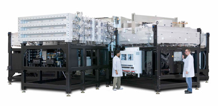
Installation for applying an insulating film on a glass surface in the manufacture of LCD screens.
In large factories, the entire process is almost completely automated - using software supplied by Applied Materials. To get some idea of the scale: a factory operating plates with a diameter of 300mm, costs in different versions from 5 to 15 billion dollars. Each installation of Applied Materials production has dimensions of the order of an office desk and costs from 2 to 6 million dollars. With an average price of 4 million, this means that there can be more than a thousand installations in one factory, and all of them are located in a clean room (several thousand square meters).
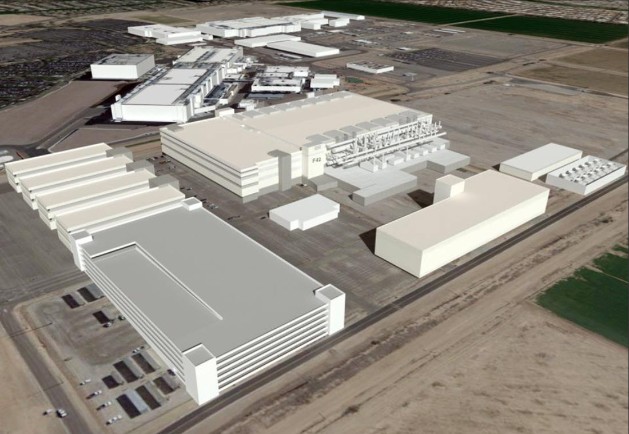
Fab 42 is an Intel factory in Arizona ($ 5 billion), construction will be completed this year.
Every whim for your money
If each manufacturing company has access to the same Applied Materials equipment, then where does this monstrous difference in the process technology come from? Why does Intel move to 22nm technology using FinFET, while Global Foundries stuck somewhere between 32nm and 45nm?
There are two reasons for this. The first, as already mentioned, Applied Materials provides the equipment, but the development of a specific process remains with the chip manufacturer or factory. Intel can use 8 layers of plating to connect transistors, and AMD only 6. Intel can detect a variant of hafnium oxide, which serves as a better dielectric than that used at TSMC, etc. Each microprocessor manufacturer uses the services of the best chemists in the world to stay on the edge of competition. And it is their job to understand the capabilities and limitations of Applied Materials equipment and get the best result with it.
The second, although Applied Materials supplies standard equipment - for $ 50 million you can buy a complete set and immediately start production using 45nm technology! But the company also works with specific manufacturers, and provides the modifications they require. If Intel needs to change the shape of one of the nozzles, or improve the piezoelectric transducer, Applied Materials will happily take on this work. Something like a trip to a car dealership: the buyer may want to force the engine or tinted glass. In essence, all cars are identical, but refined according to the wishes of customers.
Great section.
It turns out, Intel would not be able to reach the 22nm mark without close cooperation with engineers and chemists from Applied Materials. But, on the other hand, Applied Materials also knows the darkest secrets about the latest achievements of AMD. It is not difficult to imagine the scale of the conflict of interests that is taking place here. What happens if one of the engineers accidentally passes one of the secrets of FinFET technology to employees of another company?
To avoid such problems, there are separate teams in Applied Materials that work with each of the large customers and do not interact with each other. In theory, an Applied Materials engineer working with Intel will never meet an engineer working with AMD. If in the information space this is achieved by differentiating access rights and similar measures, then nothing concretely is known about the distinction that occurs in the real world. Are there separate cafeterias and working rooms for each team? And doesn't the campus of Applied Materials in Santa Clara look like a palace from a single children's book? :) Considering that Applied Materials has been working in this way for more than 40 years, they probably know how to convince their clients that they are well protected by their intellectual property.

Who remembers from which book this palace? :)
This level of collaboration and trust allows Applied Materials to enter into multibillion-dollar agreements on the creation of equipment and the exchange of intellectual property. And only because of this, 22nm, 14nm and, in the near future, 10nm are born.
22nm and more
Undoubtedly, we are already approaching the limits of the capabilities of silicon electronics (the distance between two silicon atoms is 0.5 nm). But technologies such as multi-patterning, immersion lithography and FinFET transistors make it possible to expect 14nm and 10nm processors to appear in the next few years.
As the size of transistors decreases, the accuracy of manufacturing operations increases, and hence the cost of manufacturing a single plate increases. For example, when going from 45nm to 14nm, the cost doubles due to the difficulties of creating FinFET transistors, increasing the number of metallization layers, and using multi-patterning.
With all this, Applied Materials continues to do its part of the work, increasing the yield of suitable crystals and reducing the price.
For example, the next generation of equipment will be designed for the use of plates with a diameter of 450mm. That will reduce the cost of a single microprocessor.

The growth of the diameter of the plates, the very first plates in diameter were only 25mm
Or, the creation of new approaches to the insulation of conductive bonds (inside the microprocessor, in total, there is more than 100 km of copper wire, which is responsible for 30% of the power consumption and heat generation of the crystal), which allows reducing the total CPU consumption by several percent. Not so bad if you consider that now one of the main metrics is battery life.
Here it is: Applied Materials. The unknown hero of Silicon Valley, standing on the cutting edge of semiconductor electronics, even before Intel released its first microprocessor.
Judging by the current state of affairs, experience and technology portfolio, the company is in excellent shape and is able to continue its journey to the limits of silicon electronics, and beyond.
Source: https://habr.com/ru/post/173029/
All Articles