Part 2: How to "open" the chip and what's inside? Z80, Multiklet, MSP430, PIC and others
 In this article - we continue to pick chips (and if you missed the first article - it is here ).
Under the cut - the internal K565RU5, Z80, KR580VM80A, MSP430F122, PIC16C505, PIC12C508, Russian radiation-resistant microcontroller 1886BE10, STM32F103VGT6, timer 556, the new RFID chip from Metro and Multiklet tickets.
Well, a couple of words about a more canonical method of opening the microcircuits, which leaves them in working condition.
')
The second method of opening the microcircuits
We drill with a Dremel a small depression in the center of the microcircuit:
We drop acid there (nitric or sulfuric), and heat to ~ 100 degrees. But here the usual concentrated acids are not enough - you need oleum or fuming red nitric acid. The reaction ends - wash off with acetone, dry and drop the next drop. Of course, all this must be done under the hood in protective glasses / gas mask and gloves.
We get the result - the crystal is open to our gaze, and remains operable, because the gold wire welded to the crystal remains intact. Saving operability is necessary if we want to affect the operation of the chip - either physically connect to an accessible point of the circuit, dwell with an ultraviolet laser (this way you can reset the bits in flash / eeprom memory permanently and temporarily).

We look
K565RU5G is a dynamic memory for 64 Kib , the heart of most amateur and not only computers during the Soviet era and early 90s. There was also RU7, but it was problematic to get it.

Z80A - the legendary development of the Intel 8080.
This photograph is of one of his many clones, probably produced in the GDR by MME.
The crystal size is 4950x4720 µm, technological norms are 5 µm.

KR580VM80A as KR580IK80A - analogue of the Intel 8080, mass produced in the USSR (until the mid-90s). Compared with 58080 - the area of the crystal has become less by 20%, the periphery of the crystal has been processed.
The crystal size is 4634x4164 µm, technology 5µm.

MSP430F122 - 16-bit Texas Instruments microcontroller. Remarkably, it is written on a crystal that it is MSP430F123, with a large amount of memory.

PIC12C508 is one of the “old” peaks, the production technology is 1200nm, the roughest of what was seen in microcontrollers.

PIC16C505 is another “old” peak, and again 1200nm.

A new chip from the subway tickets - before Sitronics-Micron put NXP chips into the tickets of the Moscow metro, from February of this year - Russian chips finally appeared. While I was looking for new chips - I had to check 168 metro tickets
 The new chip, compared with the NXP, is 20% smaller, but cannot be read by the NFC reader in modern cell phones.
After etching the metallization, it is clear that a substantial part of the chip is occupied by passive components (capacitors), and the places under the contact pads are empty.

The dual timer 556 is one of the oldest microchips manufactured so far.

1886BE10 is a radiation-resistant 50 MHz microcontroller developed by Milandro and manufactured at the Micron plant using 180nm technology. Resistance is achieved by the use of ring transistors and 8 transistor memory cells.

After etching the plating:

In an optical microscope, transistors do not particularly consider:

But in the electronic - everything can be seen perfectly:

Light cylinders are tungsten via remaining after etching of the layers of metallization and dielectric. This is an X-ray microanalysis - analyzes X-rays caused by the bombardment of a sample with electrons.

The STM32 STM32F103VGT6 is one of the “biggest” STMicroelectronics microcontrollers on the Cortex-M3 core.
1Mb flash memory and 96kb SRAM are placed on the chip. The crystal size is 5339x5188 µm.

180-nm static memory is again not particularly considered:

And again the electron microscope will help us:

Multiclet MCp0411100101 - as a first approximation a superscalar processor (4-wide at the moment) with an extraordinary execution of instructions, developed in Russia. Operating frequency - 100 MHz, 180nm technology.
The size of the crystal is 10.2x10.2 mm.
After etching the metallization: (Be careful, a high-resolution picture can kill your browser)

The area of the memory cell is 21.28 µm 2 . Accordingly, each of the 16 memory blocks contains 72 Kibit memory. Obviously, error correction codes (72,64) are used. The total available memory, respectively - 128 KiB.

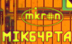
Logos:


With the crystal cut off and test areas, for example, hit the resolution test:

I hope it was interesting, this is all for now - you can subscribe to new photos in the rss-subscription .
The photos are distributed under the Creative Commons Attribution 3.0 Unported license .
Source: https://habr.com/ru/post/169687/
All Articles