Simple power monitoring device
Now more and more people are interested in the topic of monitoring the consumption of electricity.
In some cases, this knowledge is very important (for example, for your country house allocated 8kW of power and you need to understand how close you are to the allowed limit, etc.).
There are already finished products, one of them was already the hero of the review on Habré.
But we are not one of those who are looking for easy ways and will make such a device:
I got this sensor in my hands:

The remaining components will be used the most accessible and priority will be given to those that are already available.
The sensor, the photo of which is shown above, is a non-invasive current sensor (up to 100A). Sensor output - current.
Directly to the analog input of the Arduinka this sensor can not be connected (more precisely, you can, but it will not bring any benefit).
In order to obtain adequate values of the measured value, we need to add several elements and connect the sensor as follows:

The justification of the scheme and the calculation of the denominations of the elements is provided by the following link .
')
Thus, the current value can be measured, but our goal is to measure the power consumption.
We use the well-known formula: P = U * I.
And it seems that all the values in the right part are known. But, unfortunately, the voltage value can fluctuate in rather large limits and should also be measured in a good way for more accurate results.
Given this remark, we can immediately say that the device will not be very accurate and will most likely be some indicator with the ability to estimate the measured values, but with an error that also depends on the voltage value. If you have a power stabilizer installed - this error decreases.
With the connection of the sensor figured out, now we need to deal with the other components.
The ATmega168 microcircuit and the 12x2 LCD display with Cyrillic support remained from my first steps in mastering the Arduinka - and we will use them.
At the prototyping stage, it turned out that ATmega168 is, but there is no quartz with a pair of capacitors to it. But, as everyone knows, atmega can safely work at a frequency of 8 MHz with an internal oscillator.
This mode of operation is completely normal, but the accuracy of the internal oscillator is low. For the device being created this is not critical.
To enable this mode of MK, it is necessary to correct the fyuzy. Physes can be changed using the Arduino environment, but this is done only at the time of the bootloader firmware.
Components of successful firmware:
Attention, if you have an MC with an Arduinov bootloader, then you need to update the bootloader using a quartz resonator.
The firmware was successful, the MC earned on the internal oscillator.
Now I had to think about how to connect the display and buttons.
The problem is quite simple and can be connected as it is done in all examples (see links below).
The display is connected in 4-bit mode (to save used digital pins).
One of the conclusions of the display is responsible for the contrast. I wanted to be able to adjust the contrast from the sketch. Said and done: we connect this pin to a free pin with PWM (in addition we put an electrolytic capacitor at 10µF - for smoothing).
Since it was planned to use two buttons, the simplest solution would be to hang each button on your digital pin and monitor their status, but this is somehow trivial.
I decided to use only one pin for the buttons (analog).
The scheme is very simple - the buttons are turned on one after another, each resistor is parallel to each button. Consistently with this design is another resistor. This whole chain is connected between the "earth" and the "power". Thus, a voltage divider is obtained.
The feature of the circuit (and selected resistors) is such that it allows you to track the pressing of any of the buttons and the “bonus” - the fact of pressing two buttons at once, which we will use when writing a sketch.
First assembled a prototype on a solderless breadboard:

I wrote a small sketch that interrogated the sensor, made the necessary calculations and output the data to the display - everything worked as expected.
The only surprise was that the sensor, which is not connected to the wire, the current in which we want to measure, gives non-zero values - there is a small “DC component” (due to the imperfection of the elements between the sensor and the analog input of the MK). Therefore, it was decided to add a simple “autocalibration” mechanism to the sketch to eliminate it.
Now you can go to the implementation of "in the gland."
A printed circuit board for the sake of a single device, imkho, is inexpedient - I decided to do everything on a printed breadboard with a hinged installation.
For the device was purchased housing. The choice was made "by eye" (the size of the display was decisive and the fact that there should be two buttons next to it).
Photos of some components that were used in subsequent iterations:

For my own convenience, I decided to make a device of two boards.
At the top there is a display, buttons, connectors and most of the “crumbling”, referring to the display and the sensor.
On the bottom board, there is an atmega168 chip in the socket, capacitors (for power) and a connector for connecting the programmer. This board was almost empty.
To connect the boards I decided to use the pin connectors:

Of course, all the components could be placed on one board (the microcontroller should be placed under the display), but I didn’t want to do a more dense installation, and leaving the “reserve for development” is not superfluous (even if it is not needed).
"Sandwich" in the collection:

It can be seen that the boards have a "tricky" configuration - this is in order not to disturb the internal "decoration" of the acquired case. The protrusions in the body are well fixed "sandwich" inside and do not allow to hang freely in the body.
At this stage of the project, I had to think hard, how can I now mark the holes for the display, buttons and connectors, and to do it in such a way that I would not have to make a false panel?
The guides helped and the fact that the boards were made with a minimum gap - the backlash is almost zero.
Marking the necessary holes produced from the inside and used the means at hand.
He started with the buttons: he took a toothpaste and smeared the “tops” of the pushers - after that he carefully inserted the “sandwich” into the body along the guides and achieved a print on the inside of the body.
Then I drilled the holes with the drill of the required diameter using the marks obtained. And again tried on the board - bingo! The buttons were in place.
Similarly, I “smeared” the display frame (it was still under the packaging film) and repeated the manipulations. The result can be seen below.
Last "fitting", everything looks bearable:

At first, I didn’t plan to make a connector for connecting the programmer: I thought I’d make the hardware, write all the software stuffing, go and put everything together in the case, but it turned out that simply removing the connector is more convenient than disassembling the device for each software adjustment.
Programming the device using the programmer on FT232RL:

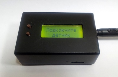
The device is assembled (though the software has not yet been added):

Demonstration of the device and its main features (here is the "final" version of the software):
I apologize for the quality - it is very inconvenient to hold the “camera” with one hand and connect, press, turn on the air conditioner, etc. with the other.
The archive with the sketch and the necessary library is available here .
I cite the links where I purchased the components. Of course, you can find cheaper.
It turns out more than 2.5 thousand rubles.
Quite a lot, but if you take only the necessary elements (and not the sets) and purchase them in the "right" places, you can save a lot (though you will have to wait longer).
Additionally, a prototype board, a set of connecting wires, a programmer , an arduinka (as an ISP programmer), etc. were used. Since these things were previously used in this "project" only temporarily - did not include them in the cost of the device created.
I also need a power supply unit for 5V (stabilized) - I did not include it in the price either, since I found it in my deposits and I don’t even know what device it was from.
As a result : another device has been created, which makes it possible to adequately assess the current electricity consumption.
The accuracy of the device is low, but when you turn on electrical consumers with known characteristics (kettle, oven, air conditioner, lamps, etc.) - the values displayed on the display correspond quite precisely to the declared by the manufacturer (an error of about 5-10%).
The device monitors both the maximum and minimum values of power consumption (it is expected that the lowest consumption was recorded at night and I had 0.58 kW - computers, network storage, a refrigerator, all sorts of charges and several devices in standby mode).
When you see the figures of current consumption - it makes you think about the efficiency of energy use and immediately want to find out, due to what you can reduce them.
PS It was already thought that the nrf24l01 + wireless module (and 3.3V power regulator for it) should be added to the “bottom” board with a MK and the device created should be converted into a “wireless sensor with a display”.
PPS about the errors found in the text please report using private messages.
In some cases, this knowledge is very important (for example, for your country house allocated 8kW of power and you need to understand how close you are to the allowed limit, etc.).
There are already finished products, one of them was already the hero of the review on Habré.
But we are not one of those who are looking for easy ways and will make such a device:
I got this sensor in my hands:
The remaining components will be used the most accessible and priority will be given to those that are already available.
Note : since the scheme is not too complicated, I will not give it entirely, but I will only tell you about some of the features.
Links to all useful materials and libraries that were used to create this device are located at the end of the article.
The sensor, the photo of which is shown above, is a non-invasive current sensor (up to 100A). Sensor output - current.
Directly to the analog input of the Arduinka this sensor can not be connected (more precisely, you can, but it will not bring any benefit).
In order to obtain adequate values of the measured value, we need to add several elements and connect the sensor as follows:
The justification of the scheme and the calculation of the denominations of the elements is provided by the following link .
')
Thus, the current value can be measured, but our goal is to measure the power consumption.
We use the well-known formula: P = U * I.
And it seems that all the values in the right part are known. But, unfortunately, the voltage value can fluctuate in rather large limits and should also be measured in a good way for more accurate results.
Given this remark, we can immediately say that the device will not be very accurate and will most likely be some indicator with the ability to estimate the measured values, but with an error that also depends on the voltage value. If you have a power stabilizer installed - this error decreases.
With the connection of the sensor figured out, now we need to deal with the other components.
The ATmega168 microcircuit and the 12x2 LCD display with Cyrillic support remained from my first steps in mastering the Arduinka - and we will use them.
At the prototyping stage, it turned out that ATmega168 is, but there is no quartz with a pair of capacitors to it. But, as everyone knows, atmega can safely work at a frequency of 8 MHz with an internal oscillator.
This mode of operation is completely normal, but the accuracy of the internal oscillator is low. For the device being created this is not critical.
To enable this mode of MK, it is necessary to correct the fyuzy. Physes can be changed using the Arduino environment, but this is done only at the time of the bootloader firmware.
Components of successful firmware:
- Arduinka with an Arduino ISP Stitched Sketch
- Arduinka with DIP-panel for the "experimental" MK (or bezdeeka mockup, where arduinka with minimal "body kit" is assembled)
- Several wires for connecting arduine (or arduinka and mock)
- The correct entry for the "new board" in the boards.txt file
Description of option in boards.txt
atmega168ic8mhz.name = ATmega168 (internal clock 8MHz)
atmega168ic8mhz.upload.protocol = stk500
atmega168ic8mhz.upload.maximum_size = 14336
atmega168ic8mhz.upload.speed = 19200
atmega168ic8mhz.upload.using = arduino: arduinoisp
atmega168ic8mhz.bootloader.low_fuses = 0xe2
atmega168ic8mhz.bootloader.high_fuses = 0xdd
atmega168ic8mhz.bootloader.extended_fuses = 0x00
atmega168ic8mhz.bootloader.path = arduino: atmega
atmega168ic8mhz.bootloader.file = ATmegaBOOT_168_pro_8MHz.hex
atmega168ic8mhz.bootloader.unlock_bits = 0x3F
atmega168ic8mhz.bootloader.lock_bits = 0x0F
atmega168ic8mhz.build.mcu = atmega168
atmega168ic8mhz.build.f_cpu = 8000000L
atmega168ic8mhz.build.core = arduino: arduino
atmega168ic8mhz.build.variant = arduino: standard
Attention, if you have an MC with an Arduinov bootloader, then you need to update the bootloader using a quartz resonator.
The firmware was successful, the MC earned on the internal oscillator.
Now I had to think about how to connect the display and buttons.
The problem is quite simple and can be connected as it is done in all examples (see links below).
The display is connected in 4-bit mode (to save used digital pins).
One of the conclusions of the display is responsible for the contrast. I wanted to be able to adjust the contrast from the sketch. Said and done: we connect this pin to a free pin with PWM (in addition we put an electrolytic capacitor at 10µF - for smoothing).
Since it was planned to use two buttons, the simplest solution would be to hang each button on your digital pin and monitor their status, but this is somehow trivial.
I decided to use only one pin for the buttons (analog).
The scheme is very simple - the buttons are turned on one after another, each resistor is parallel to each button. Consistently with this design is another resistor. This whole chain is connected between the "earth" and the "power". Thus, a voltage divider is obtained.
Drew as I could, sorry.
The feature of the circuit (and selected resistors) is such that it allows you to track the pressing of any of the buttons and the “bonus” - the fact of pressing two buttons at once, which we will use when writing a sketch.
First assembled a prototype on a solderless breadboard:
I wrote a small sketch that interrogated the sensor, made the necessary calculations and output the data to the display - everything worked as expected.
The only surprise was that the sensor, which is not connected to the wire, the current in which we want to measure, gives non-zero values - there is a small “DC component” (due to the imperfection of the elements between the sensor and the analog input of the MK). Therefore, it was decided to add a simple “autocalibration” mechanism to the sketch to eliminate it.
Now you can go to the implementation of "in the gland."
A printed circuit board for the sake of a single device, imkho, is inexpedient - I decided to do everything on a printed breadboard with a hinged installation.
For the device was purchased housing. The choice was made "by eye" (the size of the display was decisive and the fact that there should be two buttons next to it).
Photos of some components that were used in subsequent iterations:
For my own convenience, I decided to make a device of two boards.
At the top there is a display, buttons, connectors and most of the “crumbling”, referring to the display and the sensor.
On the bottom board, there is an atmega168 chip in the socket, capacitors (for power) and a connector for connecting the programmer. This board was almost empty.
To connect the boards I decided to use the pin connectors:
Of course, all the components could be placed on one board (the microcontroller should be placed under the display), but I didn’t want to do a more dense installation, and leaving the “reserve for development” is not superfluous (even if it is not needed).
"Sandwich" in the collection:
It can be seen that the boards have a "tricky" configuration - this is in order not to disturb the internal "decoration" of the acquired case. The protrusions in the body are well fixed "sandwich" inside and do not allow to hang freely in the body.
At this stage of the project, I had to think hard, how can I now mark the holes for the display, buttons and connectors, and to do it in such a way that I would not have to make a false panel?
The guides helped and the fact that the boards were made with a minimum gap - the backlash is almost zero.
Marking the necessary holes produced from the inside and used the means at hand.
He started with the buttons: he took a toothpaste and smeared the “tops” of the pushers - after that he carefully inserted the “sandwich” into the body along the guides and achieved a print on the inside of the body.
Then I drilled the holes with the drill of the required diameter using the marks obtained. And again tried on the board - bingo! The buttons were in place.
Similarly, I “smeared” the display frame (it was still under the packaging film) and repeated the manipulations. The result can be seen below.
Last "fitting", everything looks bearable:
Nervous not to look (reverse side of the board)
At first, I didn’t plan to make a connector for connecting the programmer: I thought I’d make the hardware, write all the software stuffing, go and put everything together in the case, but it turned out that simply removing the connector is more convenient than disassembling the device for each software adjustment.
Programming the device using the programmer on FT232RL:
The device is assembled (though the software has not yet been added):
Demonstration of the device and its main features (here is the "final" version of the software):
I apologize for the quality - it is very inconvenient to hold the “camera” with one hand and connect, press, turn on the air conditioner, etc. with the other.
The archive with the sketch and the necessary library is available here .
Shopping list
I cite the links where I purchased the components. Of course, you can find cheaper.
- ATmega 168 - 145 rubles.
- Current sensor - 529 rubles.
- Jack jack 3.5mm - 79 rubles. (in a set of three, only one is needed)
- Resistors and capacitors - 189 rubles. (from the set you need not all)
- Pin connectors - 319 rubles. (again, from the set you need not all)
- Power socket - 20 rubles.
- LCD display 16x2 (English-Russian) - 650 rubles.
- Clock button (h = 13mm) - 19 rubles. (2 pcs.)
- Case - 88 rubles.
- Development board - 870 rubles. (not all needed)
It turns out more than 2.5 thousand rubles.
Quite a lot, but if you take only the necessary elements (and not the sets) and purchase them in the "right" places, you can save a lot (though you will have to wait longer).
Additionally, a prototype board, a set of connecting wires, a programmer , an arduinka (as an ISP programmer), etc. were used. Since these things were previously used in this "project" only temporarily - did not include them in the cost of the device created.
I also need a power supply unit for 5V (stabilized) - I did not include it in the price either, since I found it in my deposits and I don’t even know what device it was from.
As a result : another device has been created, which makes it possible to adequately assess the current electricity consumption.
The accuracy of the device is low, but when you turn on electrical consumers with known characteristics (kettle, oven, air conditioner, lamps, etc.) - the values displayed on the display correspond quite precisely to the declared by the manufacturer (an error of about 5-10%).
The device monitors both the maximum and minimum values of power consumption (it is expected that the lowest consumption was recorded at night and I had 0.58 kW - computers, network storage, a refrigerator, all sorts of charges and several devices in standby mode).
When you see the figures of current consumption - it makes you think about the efficiency of energy use and immediately want to find out, due to what you can reduce them.
useful links
- Measuring chains
- Connection of current sensor to Arduino (selection of elements, basic formulas)
- Sketch for measuring the rms current and power
- AVR fusion calculator
- Arduino as an ISP programmer
- Connecting the LCD-display to Arduino
- Display specification and code table
- How to make a rectangular hole in the body
PS It was already thought that the nrf24l01 + wireless module (and 3.3V power regulator for it) should be added to the “bottom” board with a MK and the device created should be converted into a “wireless sensor with a display”.
PPS about the errors found in the text please report using private messages.
Source: https://habr.com/ru/post/168783/
All Articles