DipTrace and GOST. HBO Library
Something on Habré absolutely no posts about such a wonderful tool like DipTrace . I think it is necessary to correct this situation.
DipTrace is a powerful system for designing circuit diagrams and printed circuit boards (EDA - system).
Attention! Under the cut traffic!
')
DipTrace includes four main programs:
Schematic - development of schematic diagrams;

PCB Layout - PCB layout, manual and automatic tracing;

ComEdit is a case editor;
SchemEdit - component editor;

Benefits:
- Intuitive user interface ;
This statement is not accidental, since For the first time opening the GUI of this application, in the early stages I practically did not resort to reading any complicated manuals. Everything was clear on the basis of the user interface, following the prompts and menu items.
- Russian interface, help, tutorial;
Tutorial for DipTrace in Russian: www.diptrace.com/books/tutorial_rus.pdf
Really Russian support is simply wonderful. The manual has an official translation, gradually the Internet is filled with various materials about DipTrace. There is also active support in the official forum .
- Standard libraries;

Standard libraries of components simply amaze with the number of elements , libraries are actively developed and supplemented.
- Stamps compliant with GOST;
The previous version supported stamps as standard, turned out to be very useful. In the new version, why not?
- 30-day trial version and special price for the domestic market;
There is also a completely free version for 2 signal layers and 300 pins for respected radio amateurs. In principle, this is enough for small crafts.
- Special conditions for educational institutions;
There is nothing special to say, because it did not come across.
- Convenient manual and automatic positioning;
- Effective traceability;
- Comprehensive project verification;
- 3D preview of the board;
These items are just bliss compared to what P-CAD was about.
- Modeling scheme;
It is possible to unload the circuit in the Spice-model, open it and simulate it in some LT Spice.
- Import Export;
Novarm has also made sure that you do not lose your old projects. Provided the ability to import and export projects and their parts, from a number of well-known programs and formats, such as: DXF, P-CAD, PADS, OrCAD, Eagle. Netlist: Accel, Allegro, Mentor, PADS, P-CAD, OrCAD, Protel 2.0 and Tango.
- Creating files for production;
Generation (creation) of finished Gerber formats, ready for execution on CNC.
- Create your own libraries;

This is the main point of the article, we will touch it below ...
Disadvantages (in my opinion):
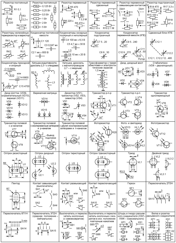
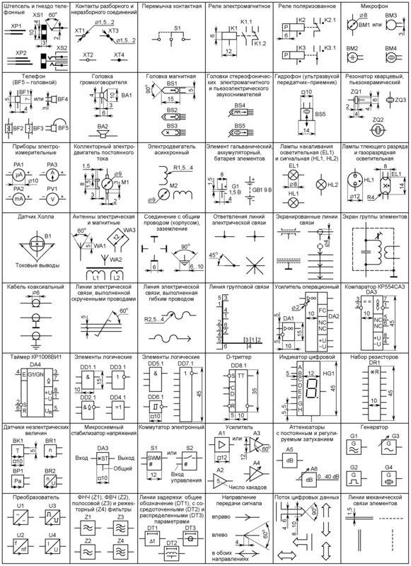
- Lack of components complying with the requirements of GOST (standard delivery);
It is strange that a part of the team and the main developers of Novarm , being our compatriots, did not implement the official releases of the UGO libraries according to GOST standards. Of course, I understand that users themselves can create what they need, and the fact that the product is mostly oriented towards European and Western audiences, but still ... I think it would contribute to the mass popularization of the product in the CIS countries, thereby creating a competition such products as P-CAD (most of which are common in Russia).
- Lack of possibility to present the list of components in the form of a tree, with strict typification by functional purpose;
With this item, I honestly do not understand. Now I will explain: the fact is that CAD itself implies a product that facilitates the development of various devices and components, of course in this case with regards to EDA systems. So: How was it possible not to implement the list of circuit elements in the form of a tree? Say it is not convenient, and would not affect performance? This question concerns actually all EDA-systems.
- Lack of printing in editors of enclosures and components;
Sometimes developed seat, I want to print and try on the component. Without printing from the case editor, it is necessary to place a newly created component in Schematic , convert it to a PCB, then print from there. Very uncomfortable.
- The absence of the possibility of arbitrary selection of the name of the list of components (by type, nominal, body, well, etc.) and the absence of a filter by components;
Those. each developer has his own preferences, for example, it is convenient for me to present the list by name and type of case, for someone it is convenient to present the list by item type (for example, MCU) and name, well, etc.
The absence of a filter by component is most likely due to the impossibility of implementing a normal filter without using a DBMS, since all components and seats are separated by files, and this is something, you understand.
- Exclusion of stamps that meet the requirements of GOST from the standard delivery;
Here it is not clear that in previous versions there were GOST stamps, in the new version they are absent. Well, let's see maybe add later.
- Lack of built-in simulator Spice-models;
I would like to, but it will be a complex product and probably expensive, so we use what we have.
Here are some answers (Novarm) to my questions:
1. While we do not plan to create a library of UGO according to the requirements of GOST, users can create components themselves according to their requirements.
2. This will require a major overhaul of the data structure until it is planned.
3. Printing in the editors of components and enclosures can be added.
4. You can search for a component in libraries by type, nominal, package, etc. We are planning to improve the search in the future.
So. Creating your own libraries:
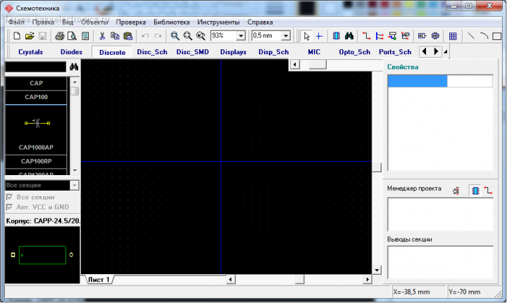
The first thing to start with is, of course, launch SchemEdit from your Start menu , or launch the application using other known methods.

Next we see the following interface:

1. The main menu area of the application;
2. Toolbar area;
3. Display area of the list of components edited by the library.
4. Working (main) application area.
5. The window of the properties of the components (in this area are indicated: the name of the component, type, dimensions, etc.).
6. Layer area. Each component consists of several layers (elements of the figure), i.e. that, from which it was created and click on one and the component layer, activates some part of it.
The next step is to set the dimension of the stage and the grid step. In my case it is:
View -> Units -> mm

and View -> Grid Size -> Custom ...

and we get: units of measurement mm , pitch (grid size) in my case 1 mm .
Next, we proceed to the creation of the component, for this we open standards, in my case it is:
and accordingly draw the selected component in the main workspace of the application.
Let the component be at Atmel ATtiny13A microcontroller (1K Flash, 64 RAM, 64 EE, 1.8 - 5.5 V, 20 MHz, ADC 4 x 10 bit), paws are called according to the Datasheet:


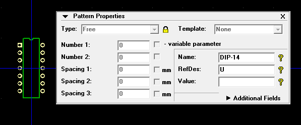
Add component footprint
click the Pattern button in the component properties window

see this window

1. Add the library (specify the path) of the component footprints, in our case it is the standard _General.lib library located along the path of the C: \ Program Files \ DipTrace \ Lib program;
2. Choose a library from the list of suggestions;
3. Choose the desired seat;
4. Check the compliance of the conclusions of the HBO template conclusions;
5. Apply changes;
Further, after the component is ready, we save it in the library. If there was no library, when trying to save a component, the application itself will offer to save the new library, you will only need to specify a name to display

and the path to where you want to keep the library

In my case it is D: \ Projects \ ESKD \ UGO \ DipTrace
Library use
Launch Schematic Editor and add the component to the schema.
To do this, open the menu item Objects -> Place Component ...
We see such a window

1. Specify the path to the library created by us;
2. Choose this library from the list of suggested ones;
3. Select the desired component;
4. Well, respectively, add it to our scheme;

Finally, the ZhogarLib library for DipTrace.
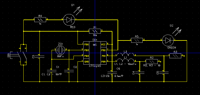
Well, for example, the scheme of the device for determining the gearshift knob - a manual gearbox (organized not on reed switches and magnets ), which I would like to talk about in my next articles.
In principle, everything, download DipTrace, install, run and use everything there is very simple.
Several resources:
Official software website: www.diptrace.com/rus/index.php
Video tour from the same Novarm: www.diptrace.com/rus/tour
Tutorial for DipTrace in Russian: www.diptrace.com/books/tutorial_rus.pdf
Some articles:
we.easyelectronics.com/tag/DipTrace
robocraft.ru/blog/technology/729.html
akvakomp.ru/manual/programs/diptrace
DipTrace is a powerful system for designing circuit diagrams and printed circuit boards (EDA - system).
Attention! Under the cut traffic!
This article (in its essence) is a reprint of my previous article published in PDF , the difference is that a bit more advantages of this CAD system are described and the process of creating a component library is described. The presented library itself is refined: everything superfluous is excluded, the library is executed in accordance with the standards of the State Standard, GOST, will be gradually updated and supplemented.
')
DipTrace includes four main programs:
Schematic - development of schematic diagrams;
PCB Layout - PCB layout, manual and automatic tracing;
ComEdit is a case editor;
SchemEdit - component editor;
Benefits:
- Intuitive user interface ;
This statement is not accidental, since For the first time opening the GUI of this application, in the early stages I practically did not resort to reading any complicated manuals. Everything was clear on the basis of the user interface, following the prompts and menu items.
- Russian interface, help, tutorial;
Tutorial for DipTrace in Russian: www.diptrace.com/books/tutorial_rus.pdf
Really Russian support is simply wonderful. The manual has an official translation, gradually the Internet is filled with various materials about DipTrace. There is also active support in the official forum .
- Standard libraries;
Standard libraries of components simply amaze with the number of elements , libraries are actively developed and supplemented.
- Stamps compliant with GOST;
The previous version supported stamps as standard, turned out to be very useful. In the new version, why not?
- 30-day trial version and special price for the domestic market;
There is also a completely free version for 2 signal layers and 300 pins for respected radio amateurs. In principle, this is enough for small crafts.
- Special conditions for educational institutions;
There is nothing special to say, because it did not come across.
- Convenient manual and automatic positioning;
- Effective traceability;
- Comprehensive project verification;
- 3D preview of the board;
These items are just bliss compared to what P-CAD was about.
- Modeling scheme;
It is possible to unload the circuit in the Spice-model, open it and simulate it in some LT Spice.
- Import Export;
Novarm has also made sure that you do not lose your old projects. Provided the ability to import and export projects and their parts, from a number of well-known programs and formats, such as: DXF, P-CAD, PADS, OrCAD, Eagle. Netlist: Accel, Allegro, Mentor, PADS, P-CAD, OrCAD, Protel 2.0 and Tango.
- Creating files for production;
Generation (creation) of finished Gerber formats, ready for execution on CNC.
- Create your own libraries;
This is the main point of the article, we will touch it below ...
Disadvantages (in my opinion):
- Lack of components complying with the requirements of GOST (standard delivery);
It is strange that a part of the team and the main developers of Novarm , being our compatriots, did not implement the official releases of the UGO libraries according to GOST standards. Of course, I understand that users themselves can create what they need, and the fact that the product is mostly oriented towards European and Western audiences, but still ... I think it would contribute to the mass popularization of the product in the CIS countries, thereby creating a competition such products as P-CAD (most of which are common in Russia).
- Lack of possibility to present the list of components in the form of a tree, with strict typification by functional purpose;
With this item, I honestly do not understand. Now I will explain: the fact is that CAD itself implies a product that facilitates the development of various devices and components, of course in this case with regards to EDA systems. So: How was it possible not to implement the list of circuit elements in the form of a tree? Say it is not convenient, and would not affect performance? This question concerns actually all EDA-systems.
- Lack of printing in editors of enclosures and components;
Sometimes developed seat, I want to print and try on the component. Without printing from the case editor, it is necessary to place a newly created component in Schematic , convert it to a PCB, then print from there. Very uncomfortable.
- The absence of the possibility of arbitrary selection of the name of the list of components (by type, nominal, body, well, etc.) and the absence of a filter by components;
Those. each developer has his own preferences, for example, it is convenient for me to present the list by name and type of case, for someone it is convenient to present the list by item type (for example, MCU) and name, well, etc.
The absence of a filter by component is most likely due to the impossibility of implementing a normal filter without using a DBMS, since all components and seats are separated by files, and this is something, you understand.
- Exclusion of stamps that meet the requirements of GOST from the standard delivery;
Here it is not clear that in previous versions there were GOST stamps, in the new version they are absent. Well, let's see maybe add later.
- Lack of built-in simulator Spice-models;
I would like to, but it will be a complex product and probably expensive, so we use what we have.
Here are some answers (Novarm) to my questions:
1. While we do not plan to create a library of UGO according to the requirements of GOST, users can create components themselves according to their requirements.
2. This will require a major overhaul of the data structure until it is planned.
3. Printing in the editors of components and enclosures can be added.
4. You can search for a component in libraries by type, nominal, package, etc. We are planning to improve the search in the future.
So. Creating your own libraries:
The first thing to start with is, of course, launch SchemEdit from your Start menu , or launch the application using other known methods.
Next we see the following interface:
1. The main menu area of the application;
2. Toolbar area;
3. Display area of the list of components edited by the library.
4. Working (main) application area.
5. The window of the properties of the components (in this area are indicated: the name of the component, type, dimensions, etc.).
6. Layer area. Each component consists of several layers (elements of the figure), i.e. that, from which it was created and click on one and the component layer, activates some part of it.
The next step is to set the dimension of the stage and the grid step. In my case it is:
View -> Units -> mm
and View -> Grid Size -> Custom ...
and we get: units of measurement mm , pitch (grid size) in my case 1 mm .
Next, we proceed to the creation of the component, for this we open standards, in my case it is:
and accordingly draw the selected component in the main workspace of the application.
Let the component be at Atmel ATtiny13A microcontroller (1K Flash, 64 RAM, 64 EE, 1.8 - 5.5 V, 20 MHz, ADC 4 x 10 bit), paws are called according to the Datasheet:
Add component footprint
click the Pattern button in the component properties window
see this window
1. Add the library (specify the path) of the component footprints, in our case it is the standard _General.lib library located along the path of the C: \ Program Files \ DipTrace \ Lib program;
2. Choose a library from the list of suggestions;
3. Choose the desired seat;
4. Check the compliance of the conclusions of the HBO template conclusions;
5. Apply changes;
Further, after the component is ready, we save it in the library. If there was no library, when trying to save a component, the application itself will offer to save the new library, you will only need to specify a name to display
and the path to where you want to keep the library
In my case it is D: \ Projects \ ESKD \ UGO \ DipTrace
Library use
Launch Schematic Editor and add the component to the schema.
To do this, open the menu item Objects -> Place Component ...
We see such a window
1. Specify the path to the library created by us;
2. Choose this library from the list of suggested ones;
3. Select the desired component;
4. Well, respectively, add it to our scheme;
Finally, the ZhogarLib library for DipTrace.
Well, for example, the scheme of the device for determining the gearshift knob - a manual gearbox (organized not on reed switches and magnets ), which I would like to talk about in my next articles.
In principle, everything, download DipTrace, install, run and use everything there is very simple.
Several resources:
Official software website: www.diptrace.com/rus/index.php
Video tour from the same Novarm: www.diptrace.com/rus/tour
Tutorial for DipTrace in Russian: www.diptrace.com/books/tutorial_rus.pdf
Some articles:
we.easyelectronics.com/tag/DipTrace
robocraft.ru/blog/technology/729.html
akvakomp.ru/manual/programs/diptrace
Source: https://habr.com/ru/post/166895/
All Articles