An inside look: RFID and other tags

Let the skyfall
When it crumbles,
We will stand tall
And face it all ...
A lot of time has passed since the publication of the last article from the beloved (at least, I really hope for it) series “Looking from the inside” - more than six months. Not that there wasn’t something to write or tell about, you just got over the cases that will be the subject of one of my next articles on Habré (I hope that it will not be sent to the scrap, as it will not be entirely dedicated to IT topics). And while there is a free minute, let's see what RFID (Radio-frequency identification) is - they will be joined by simpler tags - or as one small step in technology, it has drastically changed the lives of millions and even billions of people around the world.
')
Foreword
Immediately I would like to make a reservation.
Before starting work on this article, I really hoped that using microphotographs, and especially optics, information found on the Internet, and some baggage of knowledge from past publications will be able to determine where and what elements of the chip are located. At least at the “everyday” level: they say, this is memory, this is the power scheme, and here is the processing of information. Indeed, it would seem that RFID is the simplest device, the simplest “computer” that you can think of ...
However, life made its own corrections and everything that I managed to find: the general layout of the device of a new generation of tags , photos of how, for example, memory should look like - I don’t even know why I didn’t pay attention to this in the article about RAM (maybe opportunity to improve?), well, scandals, intrigues, exposing A5 processors from chipworks .
Part theoretical
By tradition, let's start with some introductory part.
RFID
The history of radiofrequency recognition technology — perhaps, this is what every imaginable and inconceivable RFID option (radio-frequency identification) can be called — dates back to the 40s of the 20th century, when any type of electronic technology was actively developed in the USSR, Europe and the USA .
At that time, any product that worked on electricity was still a wonder, so there was not a plowed field in front of the scientists: where you don’t stick a shovel from a shovel like in the Black Earth Region - a tree will grow. Judge for yourself: Maxwell proposed his laws only half a century ago ( in 1884 ). And theories based on these equations began to appear after 2-3 decades (between 1900 and 1914), including the theory of radio waves (from their discovery to signal modulation models, etc.). Plus, the preparation and conduct of the Second World War left their mark on this area.
As a result, by the end of the 40s, “friend-foe” recognition systems were developed, which were somewhat larger than those described in this article , but actually worked on the same principle as modern RFID tags.
The first demonstration of those close to modern RFID was held in 1973 at the Los Alamos Research Laboratory, and one of the first patents on this kind of identification system was obtained a decade later - in 1983. More information about the history of RFID can be found on the Wiki and some other sites ( 1 and 2 ).
I like the article in English more, from it you can learn a lot of useful information on use, production costs, standards, etc. etc.
In principle, any RFID tag consists of two main components - the antenna and the microchip. The antenna is needed to capture the electromagnetic waves of the transmitter (or reader), turning them:
a) in the signal
b) electricity for powering the chip itself, i.e. performing some operations, and
c) transmission of the response signal.
This is in the case of passive tags. Typically, such labels are relatively “simple” to manufacture and are used mainly in identification cards when the distance between the tag and the transmitter is minimal. The simplest example, which will be discussed in detail below, is the subway map, which exactly every day uses - even scary to think - several million people only in Moscow.
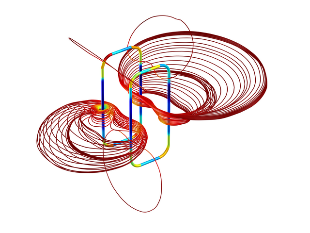
Beautiful picture illustrating the distribution of the electromagnetic field in the antennas of the reader and the card itself ( Source )
The active tags due to the built-in battery have a significantly larger radius of work, dimensions, more complicated “stuffing” (you can add a tag with a thermometer, hygrometer, and at least a whole GPS positioning chip) and an appropriate price.
Labels can be classified in different ways: by operating frequency (LF - low-frequency ~ 130KHz, HF - high-frequency ~ 14MHz and UHF - ultrahigh-frequency ~ 900MHz), according to the type of memory inside the label (read only, write once and repeatedly write). By the way, so beloved by all manufacturers and promoted by NFC belongs to the HF range, which has a number of well-known problems.
Perhaps this is where we end up with the RFID theory, especially since it seems to me somewhat boring, and who is interested in the most spicy details from the life of RFID tags - welcome! )
Other tags
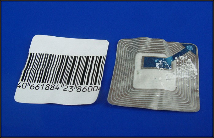
Unfortunately, the cost of RFID tags in comparison with other types of identification is quite high, so, for example, we still buy food and other “marketable” products using barcodes (or bar codes), sometimes QR codes, and against theft provide the so-called anti-theft tags (or EAS - electronic article surveillance )
The most common are three types (all photos are taken from the Wiki ):
- electromagnetic systems (usually used when selling books, they are pasted somewhere between the pages of the spine)

- acoustomagnetic systems
- radio frequency systems (usually they, or their analogues in plastic with a snap, supply clothes and bottles of elite alcohol, for example)
There are many wonderful discoveries ahead of us, sometimes completely unexpected and of course hard geek porn in HD !
If someone thought a little theory, welcome to this English-language site .
Part practical
So, what labels were found in the world around us:
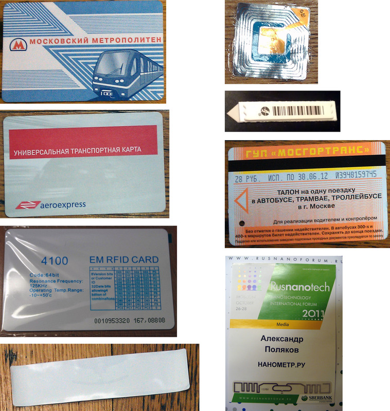
Top left column: Moscow metro map, aeroexpress travel card, plastic card for entry into the building, RFID tag presented by the Crossroads company at the exhibition RosNanoForum-2011. Top right column: radio frequency EAS tag, acousto-magnetic EAS tag, a bonus ticket for Moscow public transport with a magnetic stripe, the RFN card of the RosNanoForum visitor even contains two tags.
The first Moscow metro card is announced - let's start.
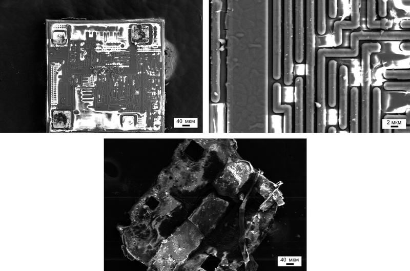
In the first circle. Moscow metro ticket
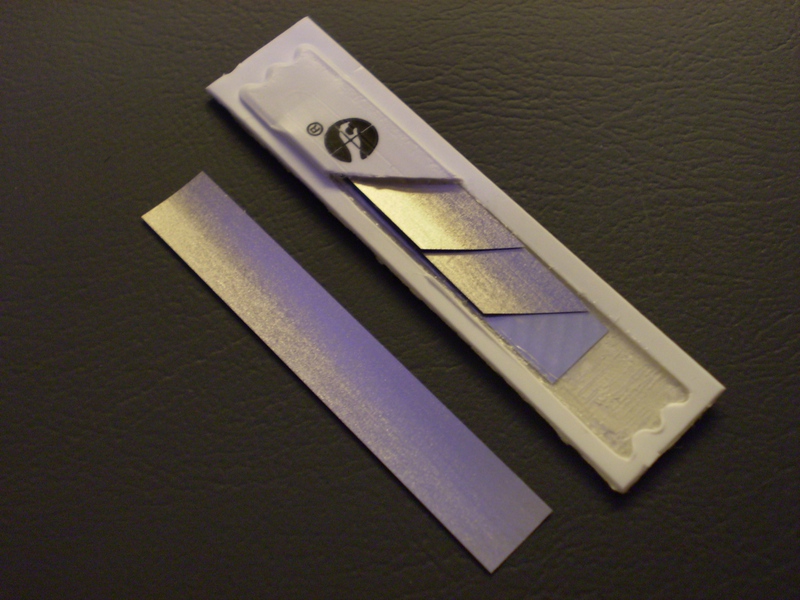
First, we soak the map in ordinary water in order to remove the paper layers that hide the very heart of this “label”.
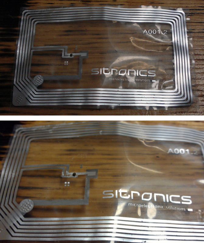
Undressed map of the Moscow metro
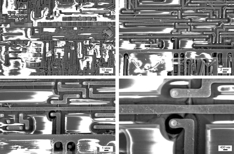
Now carefully look at it with a slight increase in the optical microscope:
Micrographs of the card chip for passage to the Moscow metro
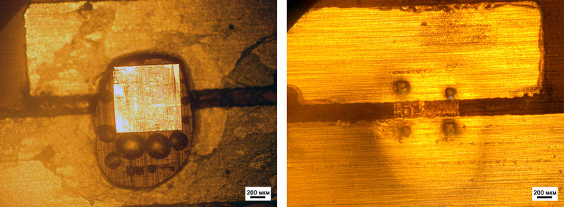
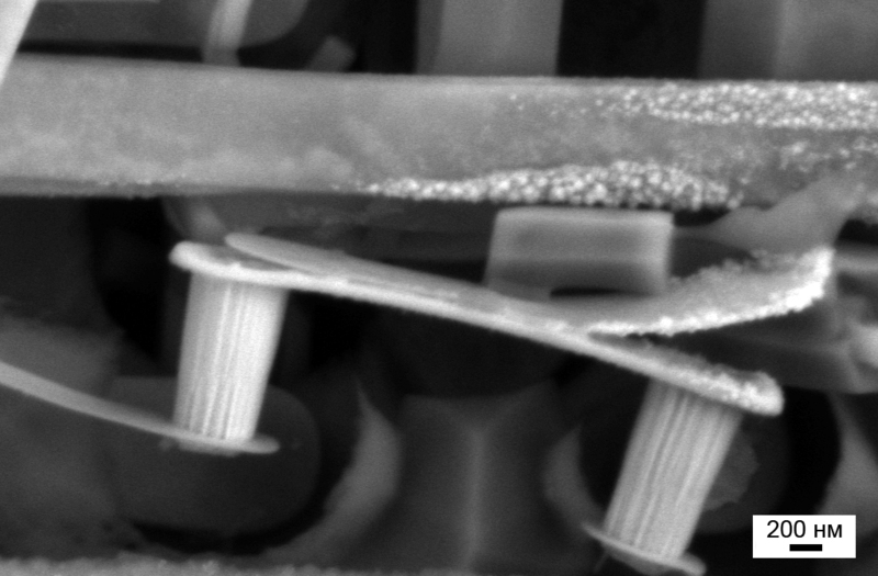
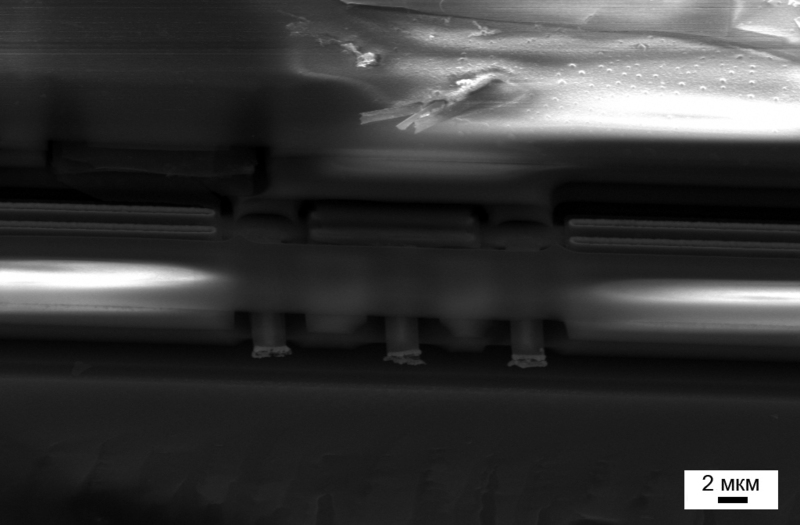
The chip is fixed quite thoroughly and I want to note that all 4 “legs” are attached to the antenna - this will be useful later for us to compare with another RFID tag. Folding the plastic base in half in the place where the chip is located, and slightly shaking from side to side, it is easily released. As a result, we have a needle-sized chip:
Optical micrographs of the chip immediately after separation from the antenna
Well, let's play around with the focus:
Changing the position of the focus from the bottom layer to the top
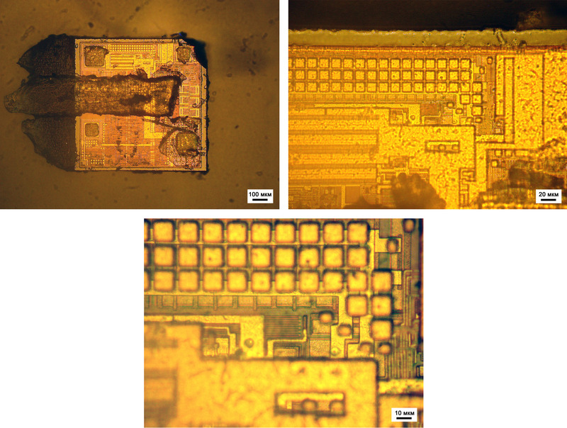
In his article on the “opening” of chips, a colleague of BarsMonster used hot acid to burn off any organic matter on the surface of the chips. I was with them a little more than affection and boiled in acetone (with reflux, of course).
NB! I strongly advise not to repeat all these sad-masochistic actions at home. BarsMonster has a “testing ground”, I have a fume hood in the laboratory.
Voila, the surface is cleaned, the last layer of metallization was not affected, and next to it is the same polymer "skin":
Purified chip and polymer base that firmly holds the chip on a plastic card
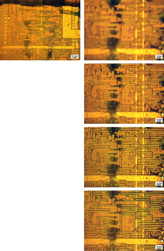
Now try to do the etching. The space between the contacts and the metallization layers must be separated by a dielectric, for example, amorphous silicon dioxide. Therefore, for etching, we take hydrofluoric acid or HF. Prepare not very concentrated solution and proceed.
After holding for 1 minute in this solution, it is difficult to notice any significant changes with an eye-armed electron microscope:
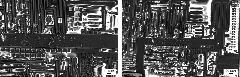
Photomicrographs of chip etching in HF after 1 minute
By the way, a very revealing photo. On it the effect of charging is well manifested and in such a contrast (charging / not charging) you can easily distinguish the individual particles of the chip from each other.
Increase the time by another 2 minutes. Since during etching it is desirable to slightly mix the solution so that the etching is more or less even, then the heaviest parts will “fly off” first:
Micrograph of the mount to the antenna, detached from the chip
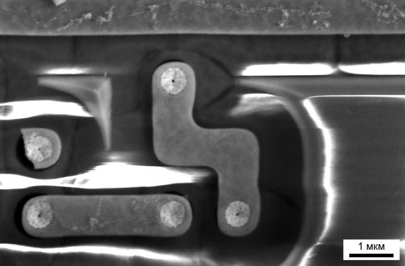
Take a look at a different angle
And here is the place of attachment sites. In some places the pins are torn out, and in some places they remain untouched:
About sizes. The thickness of the metal deposition in the chip can range from 20-30 nm to 100-150 nm, while the distance between the metallization layers, judging by the photos presented above, is about 950 nm. It turns out that very thin and tense (this is due to the conditions of application of these conductors) metal “films” stand on a massive “barrel”, therefore, when the acid eats away the carrier base - silicon dioxide, the films try to relieve tension, and massive contacts between the metallization layers "Fall" on the vacated space under them. It is the dimensions of the elements and some of the limitations of the experiments that do not allow the dielectric to be carefully etched out and look at the 3D grid of conductors between the individual chip elements.
Sometimes science turns a little into art, for example, in this way:
Nanoscalee ...
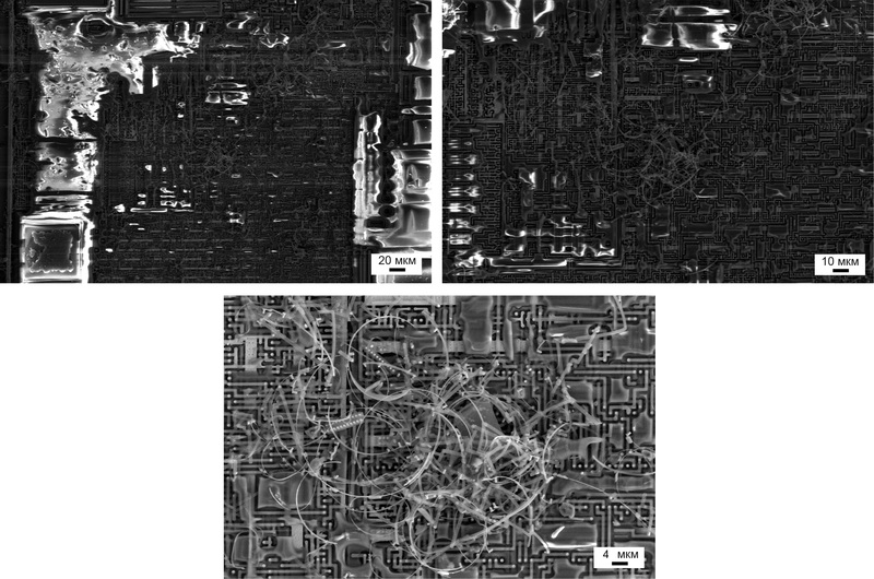
Let stand another couple of minutes in hydrofluoric acid (a total of 5 minutes already). The landscape is beginning to change dramatically - more and more parts are leaving their places. Anarchy is coming:
General view of the chip after a total of 5 minutes of etching
In addition to everything else, we maintain the chip in acid, which means whether we like it or not, but the metal will interact with the acid, gradually dissolving. As was shown in the article about the matrix of cameras using EDX-analysis, manufacturers extremely do not like to shell out for gold and use cheaper aluminum. It would seem that an oxide film should form on the surface of such a metal, however, because of the production technology, there is practically pure aluminum inside the chip.
After another 2 minutes of aging, another feature of the etching process, the uniformity, begins to manifest itself. Gradually removed layer by layer equally over the entire surface, which means that the places where the two layers of metallization come in contact are etched in the same way as the rest of the surface. As a result, we have bagels around contacts:
Bagels around contacts between plating layers
Another clear proof of this is the “knocked out” whole contact groups:
We uproot contact groups ...
The solvent penetrates into these holes, as we remember, slightly increases the metal and etches the space through separate layers of metallization - something like this:
Micrograph of a pickled chip showing two separate dielectrics with a cavity between them.
From another angle, in order to leave no doubts, these are really two different layers of silicon dioxide, and under, between, above and around them are layers of metallization.
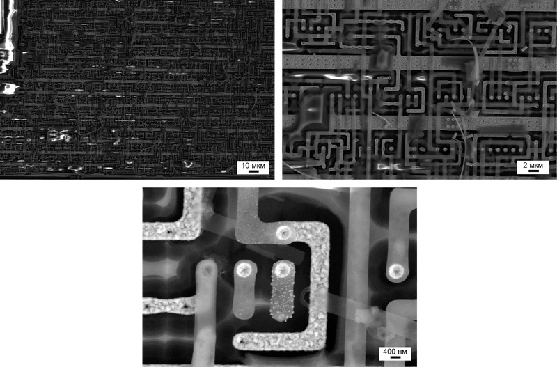
Another fun discovery is three outputs that, apparently, when testing chips on a plate after the end of the production cycle for rejection:
Three "test" output from the chip
Since after the exhibition at the Festival of Science 2012 in the building of the Fundamental Library of Moscow State University, I am drawn to art, I can’t deny myself the pleasure of sharing with you a nanotretris:
Let's play tetris?
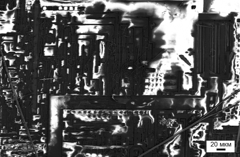
And we will deal a decisive blow to this chip by placing it in the etching solution for another 7 minutes (total, 14 minutes from the beginning of the experiment, which stretched for almost a whole day of work;)). Only the first layer of metallization remained on the surface, drains, sources and gates are already beginning behind it:
Throughout the mess, you can find and order - than you last photo is not a new emblem for Habr?
The first, the main layer of metallization, followed by only transistors ...
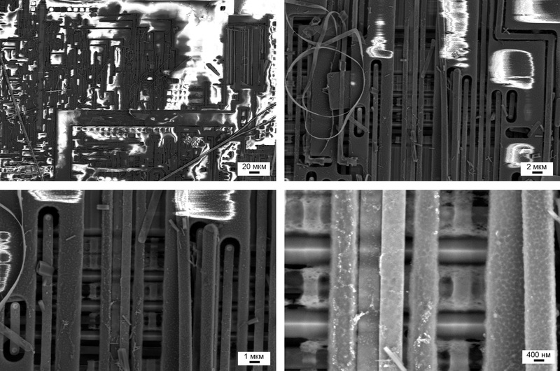
Well, take a look in a retrospective view of what path we have taken in the process of etching the chip:
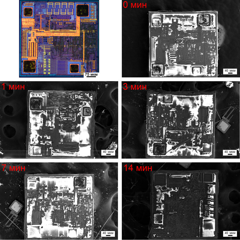
General micrographs illustrating the etching process
Oh yes, I promised geek porno in HD. Thank you for this BarsMonster and its long-focus microscope:
Picture is clickable - HD
Now a little intrigue.
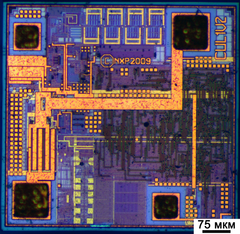
It is rumored that Micron develops and produces chips for the Moscow metro of its own forces using similar Mifare technology (at a minimum, the attachment to the antenna is different - the legs of a different shape). On August 22, BarsMonster,
The ticket discussed above seems to have been manufactured (or just mounted on an antenna?) At the Micron plant (Zelenograd) - see links below - using the technology known in NXP's RFID circles, which are actually hinted at by 3 huge letters and year of technology (and maybe year of production) on the top layer of the chip metallization. If we assume that 2009 refers to the launch year of the technology, and the abbreviation CUL1V2 is decoded as Circuit ULtralite 1 Version 2 (this assumption is also confirmed by this news ), then on the NXP website you can find a detailed description of these chips (the last two lines are listed )
By the way, last year, an excursion to the Micron plant was organized for the participants of the Internet Olympiad on Nanotechnologies ( photo and video reports), so there is no sense to say that the equipment there is idle, but the statement “uncle in a white coat” that they make tags By standards 70 nm, I would question ...
According to the statistics collected by BarsMonster after analyzing the chips of 109 metro tickets (a fairly representative sample), according to the normal distribution, the chances of finding an “unusual” ticket are ~ 109 ^ 1/2 or about 10%, but they melt with every ticket opened ...
The English-language Wiki website has an adorable Mifare article, which presents a rather incomplete, but rather extensive list of where and what types of data labels are used.
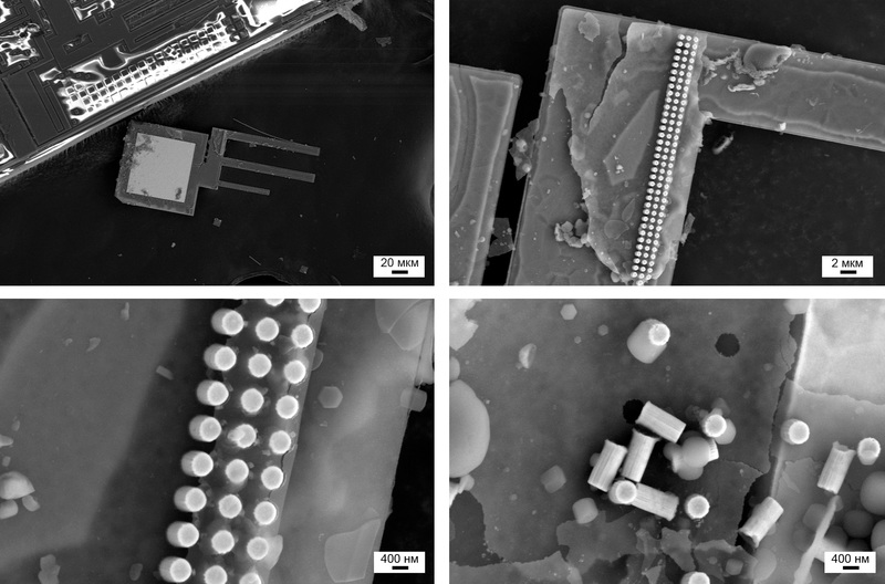
In the second circle. Aeroexpress Ticket
The ticket queue, which is used by many, goes to other cities of our vast Motherland or abroad through the air gates of Moscow, Sochi or Vladivostok (I think that only these three cities now have Aeroexpress).
Since the chip is practically no different from Mifare, which is used in the Moscow metro, let's start with hardcore:
Focus on the first plating layer (Image is clickable - HD)
Focus on the last plating layer (Picture is clickable - HD)
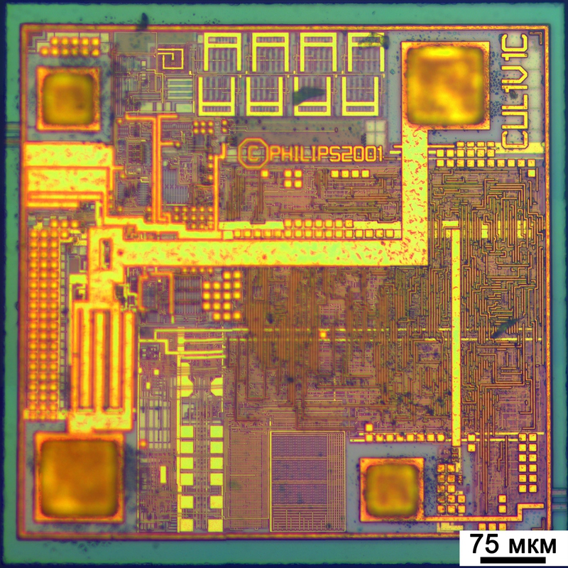
A close look has already noticed the main difference between the two Mifare chips - the inscription Philips2001. In fact, back in 1998, the Philips company bought the American manufacturer of microelectronics - Mikron (not to be confused with our Zelenograd Micron). And in 2006, NXP sprang from Philips.
It is also easy to see the mark CLU1V1C, which, based on the above, means Circuit ULtralite 1 Version 1C. That is, this label is the predecessor of Mifare, used by the Moscow metro, and, therefore, compatible with it on the main parameters. However, as in the previous case, 2001 is an indication of the year of development and implementation of the technology or the year of production. It's strange that Aeroexpress uses outdated tags ...
In the third circle. A plastic card
Once, I decided to show articles and photos to Habrahabr to one of my friends. Then he asked if she had any unnecessary map for the next RFID article. By that time, she had just moved to study at the EPFL and presented me with a card, which is being passed to one of the buildings of Moscow State University. The map, respectively, without any marking, and I'm not even sure that it contains at least something other than the usual key to enter the building.
The card is completely plastic, so we immediately put it in acetone for just a few tens of minutes:

We take acetone baths
Inside, everything is pretty standard - the antenna and the chip, though, he was on a small piece of PCB. Unfortunately, without any identification marks - the typical Chinese noname. The only thing that can be learned about this chip and card is that they are manufactured / belong to some standard TK41. Such cards are full of sales like ali-baba and dealextreme.
Picture is clickable - HD
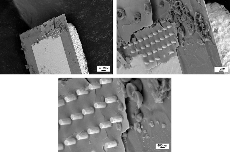
In the fourth circle. Crossroads
Next, I want to consider two tags presented at the exhibition RosNanoForum 2011. The first of them presented with great pathos, saying that this is almost a panacea for thieves and thefts in stores. Anyway, this label will allow you to fully transfer stores to self-service. Unfortunately, the effective manager turned out to be a little more than completely incompetent in matters of school physics. And after the proposal to check the effectiveness of it and the label with a strong magnet attached to the label, quickly hushed up the topic ...
After a couple of purchases in SmartShop, I have a few tags left. Clearing one of them from glue and a white protective layer we see the following:
New label of the Perekrestok chain of stores
We proceed in the same way as Mifare and carefully detach it from the polymer base and antenna and place it on the table of the optical microscope:
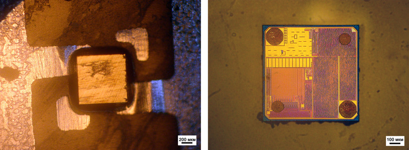
Optical micrographs of the label to be used in SmartShop
By happy coincidence (either the glue was pumped up, or so conceived), the tag was removed from the base quickly, and its surface remained without any traces of glue. I would like to note that if Mifare has all 4 contacts attached to the antenna (2 contacts at each end), then we see that two contacts are connected to two small areas that are not in contact with the antenna.
Let's play a little with focus in different parts of the label:
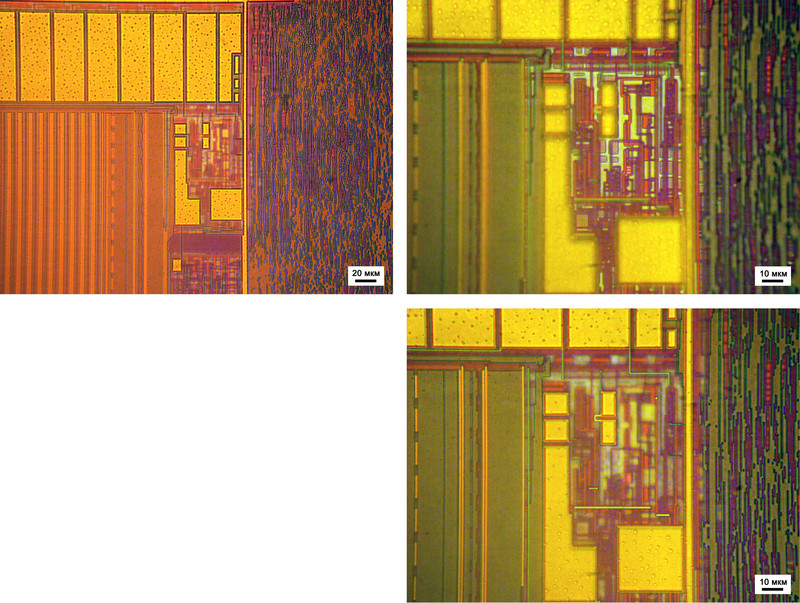
Change the focus ...
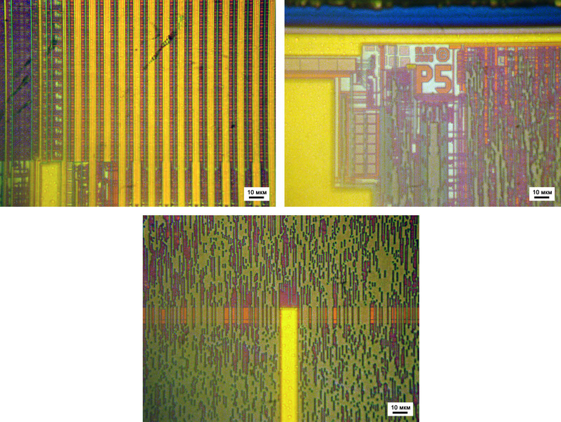
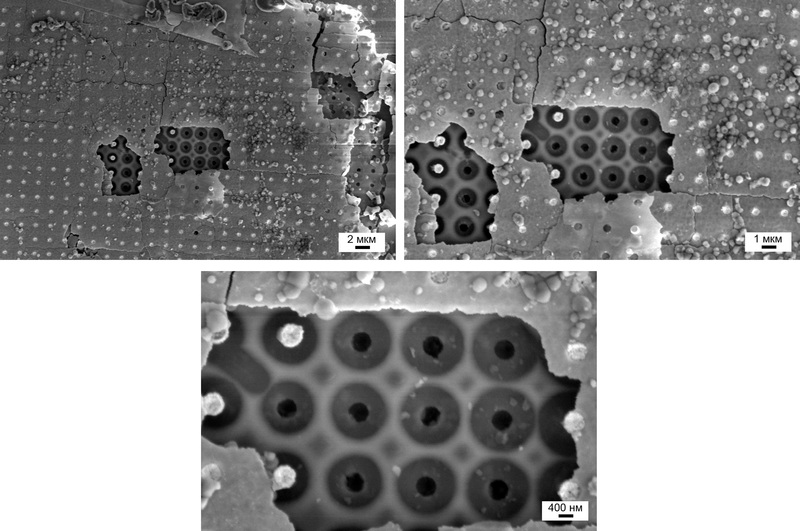
Maximum magnification optical microscope
In the last photo on the left above, apparently, the EEPROM memory module is captured, as it occupies about a third of the chip surface and has a “regular” structure.
Picture is clickable - HD
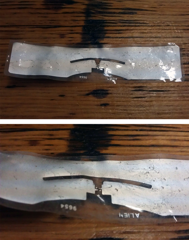
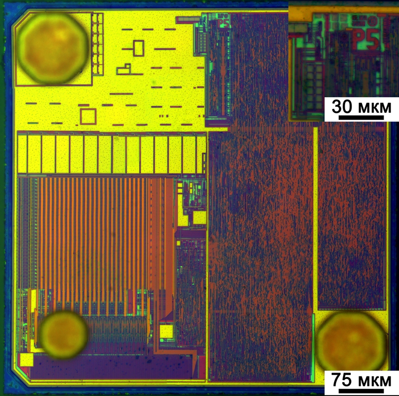
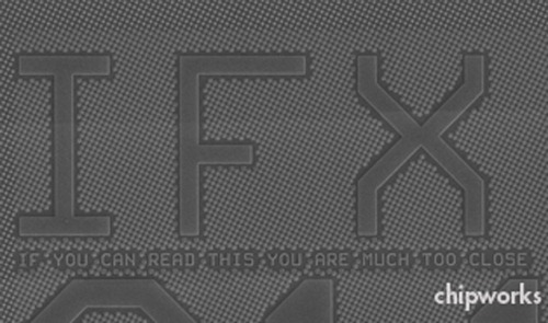
This label maker strenuously hides their origin. Agree, the size of this remarks “P5 Alien” is several times smaller than the inscription “NXP” or “Philips”. It reminds me of a light trolling from Samsung, which was noticed by the guys from the chipworks after the opening of the Galaxy S and called "silicon art":
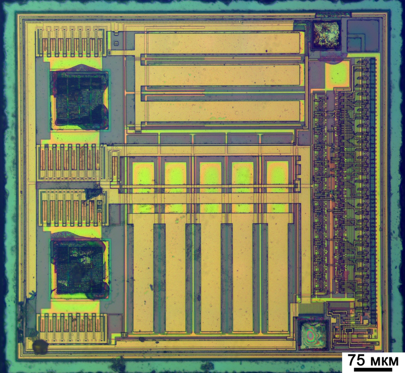
But back to our label. Searches on the Internet led to two sites - Wiki and the manufacturer Alien Tech . After a little wandering around the company's website, the type of tag — Higgs 3 and the full specification for it — is very quickly located.
Higgs 3 refers to the EPC gen2 standard. More information is always available on here .
In the fifth circle. Tags used in the badges of RosNanoForum
For sweets, I saved the tags that were used for identification at RosNanoForum in 2011. As can be seen from the photo below, the badge is not simple, but has two labels - one in sight (narrow at the bottom), and the second is hidden inside.
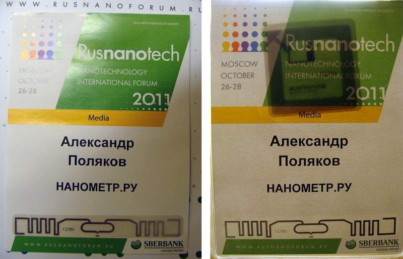
Unfortunately, the big tag is the usual Mifare, absolutely the same one used in the Moscow metro, but the small one is slightly different from everything we saw earlier: The
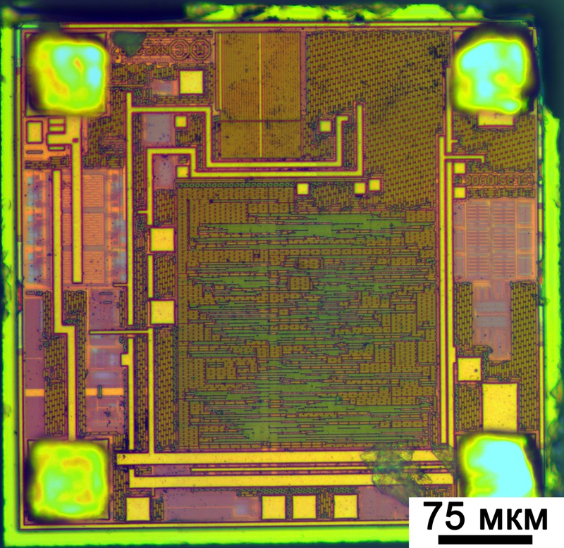
picture is clickable - HD
This is a RFID tag from NXP, but of a different standard than Mifare and much less, and released in 2007. The name that is read to the right is t5 (S?) L35 (S?) 10V0 (O?) E. But it could not be deciphered ...
Bonus
1. Yes, we completely forgot about the magnetic card used to pay for travel in public transport in Moscow - correct: The

bright dots in the bottom photo can be just particles of magnetic material used to record information on the card.
2. Two words about NFC. In the summer, a rather interesting article was published on the development of NFC in Russia, albeit at 2.4 MHz.
3. By the way, the RFID store is already open - you can try it ...
PS: The author is grateful to the BarsMonster user , who, by the way, can also be congratulated on the successful translation of the article into English , which your humble servant has yet to do ... and they are still a dozen - OMG!
PPS: Not so long ago an article was published on the 3DNews website, devoted to the study of displays of various top and not-so devices. If you have not yet decided to choose a smartphone, then you are right here ...
First , the full list of published articles on Habré:
Opening the Nvidia 8600M GT chip , a more detailed article is given here: Modern chips - a view from the inside
An inside look: CD and HDD
An inside look: LED bulbs
An inside look: the LED industry in Russia
An inside look: Flash and RAM
An inside view: the world around us
Inside View: LCD and E-Ink Displays
An inside look: matrix digital cameras
An inside look: Plastic Logic
An inside look: RFID and other tags
An inside look: postgraduate study at EPFL. Part 1
An inside look: postgraduate study at EPFL. Part 2
An inside view: the world around us - 2
An inside view: the world around us - 3
View from the inside: the world around us - 4
and 3DNews:
Microview: a comparison of modern smartphones displays
Secondly , in addition to the blog on HabraHabr , articles and videos can be read and viewed on Nanometer.ru , YouTube , and Dirty .
Thirdly , if you, dear reader, liked the article or you want to stimulate the writing of new ones, then act according to the following maxim: “pay what you want”
Yandex.Money 41001234893231
WebMoney (R296920395341 or Z333281944680)
Sometimes briefly, and sometimes not so much about the news of science and technology, you can read on my Telegram channel - welcome;)
Source: https://habr.com/ru/post/161401/
All Articles