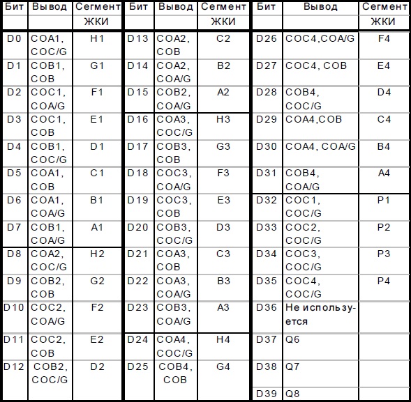
MSP430 + LCD from “Minik 1101F”
Like my colleagues writing articles with the “MSP430” tag, my acquaintance with this microcontroller began with a note from the Texas Instruments based MSP430 developer kit . Ordered kit arrived in 5 days. Then the LED “Hello, World” and ... was put in the cabinet for lack of ideas and time ...
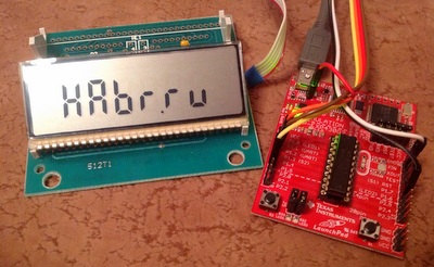
... But once in the warehouse were found unused cashbox "Minika 1101F." From childhood, the familiar question “what’s inside?” Did its job :)
Inside, the LCD indicator IZhTS13-8 / 7-01 was detected on the board with magic numbers 5.104.704.
This is what this board looks like.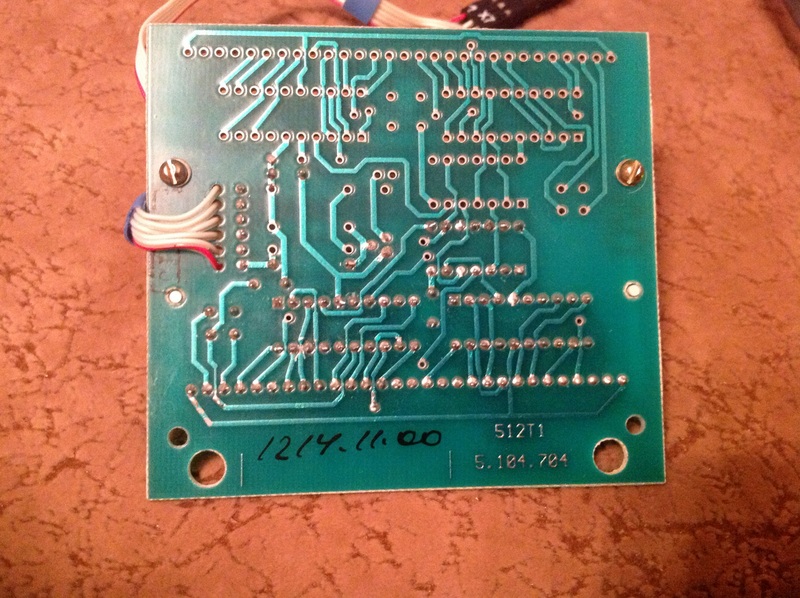
Scrolling through the thematic forums stumbled upon a circuit board concept .
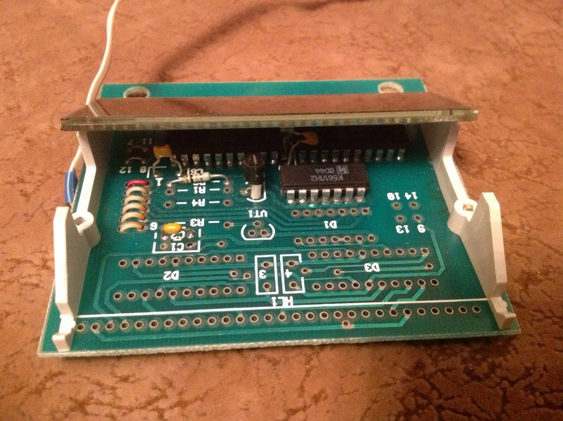
The board is two-sided, consists of 2 KR1820VG1 microcircuits (yes, everything is correct, two of them are on the 4-re circuit, but a list of elements that are not installed on the board is given). This microcircuit is a complete analogue of the Texas Instruments COP472-3 microcircuit. I bring datasheet . Once again I was surprised that the Soviet (or Russian?) Designers even cloned that !
Each microcircuit is able to control 4 digital digits of the indicator (this indicator has 8 digits for this indicator). Therefore, one of the microcircuits is responsible for 4 senior digits, and the other for 4 low bits.
Also, the engineers “let through” all the signals through the inverters assembled in the notorious K561LN2 (I didn’t understand why, because it was more convenient for the already developed earlier circuit of the central cash register unit).
Connection
The LCD module was connected to the main board of the cash register with a 6-pin connector X7. Here I had to double-check the order in which the contacts on the connector are located.
I looked where the conductors were going and drew the connection diagram for the MSP430.
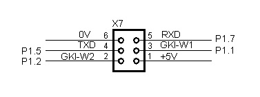
Ports MSP430G2553 will be involved next. in the following way:
- P1.1 - the choice of the younger crystal
- P1.2 - the choice of the highest crystal
- P1.5 - sync pulse
- P1.7 - data
Algorithm
The algorithm of operation of the KR1820VG1 microcircuits is well described in the well-known 1990 article of Leonid Ivanovich Ridico Automobile clock-thermometer-voltmeter . Also on the Internet there was a useful scan of the magazine ELECTRONICS: Science, Technology, Business 5/2007 .
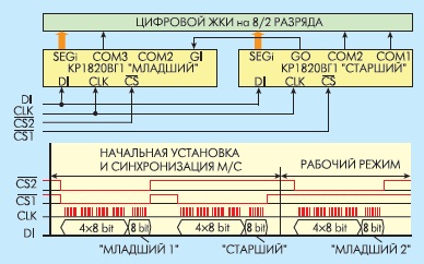
The following picture shows the operation of two IC KR1820VG1 in the cascade mode. This is exactly what is used here.
')
Sets of service bits here are ingeniously named "JUNG1 / 2" and "SENIOR".

We describe the algorithm of VG1 in a cascade. It would be possible to write the “algorithm of the board operation”, but that would not be true - do not forget that we have soldered inverters to all the board inputs .
Work consists in 1) initialization and 2) in fact, the operating mode.
Initialization occurs trail. in the following way:
1) on both chips we put ^ CS1,2 = 0;
2) give 32 bits of data to the D line;
3) we give 4 bits of special segments (in this indicator these are lines above the numbers);
4) issue 4 control bits 0111 (see tab. "LESS1");
5) on both chips we put ^ CS1,2 = 1;
6) choose the high-end chip ^ S2 = 0, it will now receive the data;
7) give 32 bits of data to the D line; issue 4 bits of special segments; issue 4 control bits 1000 (see table. “SENIOR”);
8) ^ CS = 0.
Initialization code looks like this
/* * LCD */ void initLCD(){ P1OUT |= CS1+CS2; // ~CS "0" // ( - , "1") // spi_IO(0); spi_IO(0); spi_IO(0); spi_IO(0); // 4 spi_IO(0x07); // 4 + 4 P1OUT &= ~(CS1 + CS2); // ~CS=1 ( ) P1OUT |= CS2; // ~CS=0 - spi_IO(0); spi_IO(0); spi_IO(0); spi_IO(0); // 4 spi_IO(0x08); // 4 + 4 P1OUT &= ~(CS2 + CS1); // ~CS=1 (!) } Any useful features
/* "1" */ void bit1() { P1OUT &= ~D; P1OUT &= ~CLK; P1OUT |= CLK; } /* "0" */ void bit0() { P1OUT |= D; P1OUT &= ~CLK; P1OUT |= CLK; } /* */ void spi_IO( unsigned int data ) { unsigned int i; for( i = 0; i < 8; i++ ) { // if( data & 0x80 ) bit1(); else bit0(); data <<= 1; } } The chip goes into operation.
Now, in order to write data to high / low 4 digit (i.e. to high / low chip), you can simply select the desired chip and write directly to it.
Work mode:
1) select the desired chip (younger ^ CS1 = 0 or older ^ CS2 = 0);
2) send 32 bits of data;
3) send 4 bits of special segments;
4) send 4 control bits (0110 for the younger “JUNIOR 2” or 1000 for the older one);
5) “pick up” the chip (the one in item 1. Selected = 1).
Please do not judge strictly for the track. a piece of code. You can optimize and optimize, but the purpose of the article is not in this :)
Implementing character string display
/* * * data - * n - * dot - () */ void print_LCD( char data[], char n, char dot ) { unsigned char copy[8]; unsigned char i; if(n<1) return ; if(n>8) n=8; for( i = 0; i < 8; i++ ) if(i+1>n) copy[i] = ' ' ; else copy[i] = data[i]; // // 4 P1OUT |= CS1; for(i=0;i<4;i++){ if( dot & 0x80 ) spi_IO(char2byte(copy[i])+0x80); else spi_IO(char2byte(copy[i])); dot <<= 1; } // 4 , ( ) bit0(); bit0(); bit0(); bit0(); // bit0(); bit1(); bit1(); bit0(); P1OUT &= ~CS1; // 4 P1OUT |= CS2; for(i=4; i<8; i++){ if( dot & 0x80 ) spi_IO(char2byte(copy[i])+0x80); else spi_IO(char2byte(copy[i])); dot <<= 1; } // 4 , ( ) bit0(); bit0(); bit0(); bit0(); // bit1(); bit0(); bit0(); bit0(); P1OUT &= ~CS2; } Now we can highlight individual segments. But this is not really interesting, so we need a character generator!
Sign generator
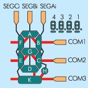
In this picture we see the sequence of bits in the code message (see item 2 of the algorithm).
And on this one there is a typical LCD layout layout (on our, however, “K” above the number, and here - under).
In the character generator code, everything through the case, I apologize :)
Character generator code
/* * */ int char2byte( char ch ){ switch(ch){ case '1' : return 0x06; case '2' : return 0x5B; case '3' : return 0x4F; case '4' : return 0x66; case '5' : return 0x6D; case '6' : return 0x7D; case '7' : return 0x07; case '8' : return 0x7F; case '9' : return 0x6F; case 'O' : case 'o' : case '0' : return 0x3F; case 'a' : case 'A' : return 0x77; case 'b' : case 'B' : return 0x7C; case 'c' : case 'C' : return 0x39; case 'd' : case 'D' : return 0x5E; case 'e' : case 'E' : return 0x79; case 'f' : case 'F' : return 0x71; case '-' : return 0x40; case ' ' : return 0x00; case 'p' : case 'P' : return 0x73; case 'g' : case 'G' : return 0x31; case 'l' : case 'L' : return 0x38; case 'h' : case 'H' : return 0x76; case 'y' : case 'Y' : return 0x38; case 'r' : case 'R' : return 0x50; case 'u' : return 0x1C; case 'U' : return 0x3E; case '|' : return 0x30; case '~' : return 0x01; // case '_' : return 0x08; // case '=' : return 0x09; // case 'j' : return 0x21; // ( - // jkmn ) case 'k' : return 0x03; // case 'm' : return 0x0C; // case 'n' : return 0x18; // default: return 0x00; } } Further several demo functions were written, which can be viewed at the link at the end of the article.
Afterword
The LCD fee is powered by 5V. On the MSP430 Launchpad, only 3.3V are separated. From them the fee works too, but very dimly. Probably, the required brightness can be achieved by selecting the R3 * resistor, but soldering the pin at the USB input and removing 5V from it also works :) In the end, we do not have a complete product, but a laboratory layout.
I also note that on this board, the older 4 segments of the numbers are located on the right, and the younger ones are on the left .
The full firmware code can be downloaded here or
look
Nervous in the code I advise you not to look :) #include <msp430g2553.h> #define CS1 BIT1 // #define CS2 BIT2 // #define CLK BIT5 // #define D BIT7 // char flag_next=0; // ( ) /* "1" */ void bit1() { P1OUT &= ~D; P1OUT &= ~CLK; P1OUT |= CLK; } /* "0" */ void bit0() { P1OUT |= D; P1OUT &= ~CLK; P1OUT |= CLK; } /* * ( ) */ void delay( unsigned int ms) { while (ms--) __delay_cycles(16000); } /* */ void spi_IO( unsigned int data ) { unsigned int i; for( i = 0; i < 8; i++ ) { // if( data & 0x80 ) bit1(); else bit0(); data <<= 1; } } /* * */ int char2byte( char ch ){ switch(ch){ case '1' : return 0x06; case '2' : return 0x5B; case '3' : return 0x4F; case '4' : return 0x66; case '5' : return 0x6D; case '6' : return 0x7D; case '7' : return 0x07; case '8' : return 0x7F; case '9' : return 0x6F; case 'O' : case 'o' : case '0' : return 0x3F; case 'a' : case 'A' : return 0x77; case 'b' : case 'B' : return 0x7C; case 'c' : case 'C' : return 0x39; case 'd' : case 'D' : return 0x5E; case 'e' : case 'E' : return 0x79; case 'f' : case 'F' : return 0x71; case '-' : return 0x40; case ' ' : return 0x00; case 'p' : case 'P' : return 0x73; case 'g' : case 'G' : return 0x31; case 'l' : case 'L' : return 0x38; case 'h' : case 'H' : return 0x76; case 'y' : case 'Y' : return 0x38; case 'r' : case 'R' : return 0x50; case 'u' : return 0x1C; case 'U' : return 0x3E; case '|' : return 0x30; case '~' : return 0x01; // case '_' : return 0x08; // case '=' : return 0x09; // case 'j' : return 0x21; // ( - // jkmn ) case 'k' : return 0x03; // case 'm' : return 0x0C; // case 'n' : return 0x18; // default: return 0x00; } } /* * * data - * n - * dot - () */ void print_LCD( char data[], char n, char dot ) { unsigned char copy[8]; unsigned char i; if(n<1) return ; if(n>8) n=8; for( i = 0; i < 8; i++ ) if(i+1>n) copy[i] = ' ' ; else copy[i] = data[i]; // // 4 P1OUT |= CS1; for(i=0;i<4;i++){ if( dot & 0x80 ) spi_IO(char2byte(copy[i])+0x80); else spi_IO(char2byte(copy[i])); dot <<= 1; } // 4 , ( ) bit0(); bit0(); bit0(); bit0(); // bit0(); bit1(); bit1(); bit0(); P1OUT &= ~CS1; // 4 P1OUT |= CS2; for(i=4; i<8; i++){ if( dot & 0x80 ) spi_IO(char2byte(copy[i])+0x80); else spi_IO(char2byte(copy[i])); dot <<= 1; } // 4 , ( ) bit0(); bit0(); bit0(); bit0(); // bit1(); bit0(); bit0(); bit0(); P1OUT &= ~CS2; } /* * LCD */ void initLCD(){ P1OUT |= CS1+CS2; // ~CS "0" // ( - , "1") // spi_IO(0); spi_IO(0); spi_IO(0); spi_IO(0); // 4 spi_IO(0x07); // 4 + 4 P1OUT &= ~(CS1 + CS2); // ~CS=1 ( ) P1OUT |= CS2; // ~CS=0 - spi_IO(0); spi_IO(0); spi_IO(0); spi_IO(0); // 4 spi_IO(0x08); // 4 + 4 P1OUT &= ~(CS2 + CS1); // ~CS=1 (!) } /* * */ void clear_LCD() { print_LCD( " " , 8, 0); // - } /* * */ void demo() { int demo_n = 1; while(1){ switch(demo_n){ case 0:{ int ms=50; while(1){ print_LCD("~~ " ,8,0); delay(ms); print_LCD(" ~~ " ,8,0); delay(ms); print_LCD(" ~~ " ,8,0); delay(ms); print_LCD(" ~~ " ,8,0); delay(ms); print_LCD(" ~~ " ,8,0); delay(ms); print_LCD(" ~~ " ,8,0); delay(ms); print_LCD(" ~~" ,8,0); delay(ms); print_LCD(" k" ,8,0); delay(ms); print_LCD(" 1" ,8,0); delay(ms); print_LCD(" m" ,8,0); delay(ms); print_LCD(" __" ,8,0); delay(ms); print_LCD(" __ " ,8,0); delay(ms); print_LCD(" __ " ,8,0); delay(ms); print_LCD(" __ " ,8,0); delay(ms); print_LCD(" __ " ,8,0); delay(ms); print_LCD(" __ " ,8,0); delay(ms); print_LCD("__ " ,8,0); delay(ms); print_LCD("n " ,8,0); delay(ms); print_LCD("| " ,8,0); delay(ms); print_LCD("j " ,8,0); delay(ms); if(flag_next==1) { demo_n=1; flag_next=0; break; } } } case 1:{ clear_LCD(); while(1){ print_LCD( " H" , 8, 0); delay(200); print_LCD( " HE" , 8, 0); delay(200); print_LCD( " HEL" , 8, 0); delay(200); print_LCD( " HELL", 8, 0); delay(200); print_LCD( " HELLO", 8, 0); delay(200); print_LCD( " HELLO ", 8, 0); delay(200); print_LCD( " HELLO ", 8, 0); delay(1000); print_LCD( "HELLO ", 8, 0); delay(200); print_LCD( "ELLO ", 8, 0); delay(200); print_LCD( "LLO " , 8, 0); delay(200); print_LCD( "LO " , 8, 0); delay(200); print_LCD( "O " , 8, 0); delay(200); print_LCD( " H" , 8, 0); delay(200); print_LCD( " HA" , 8, 0); delay(200); print_LCD( " HAB" , 8, 0); delay(200); print_LCD( " HABR", 8, 1); delay(200); print_LCD( " HABRR", 8, 2); delay(200); print_LCD( " HABRRu", 8, 4); delay(200); print_LCD( " HABRRu ", 8, 8); delay(1000); print_LCD( "HABRRu ", 8, 16); delay(200); print_LCD( "ABRRu ", 8, 32); delay(200); print_LCD( "BRRu ", 8, 64); delay(200); print_LCD( "RRu " , 8, 128); delay(200); print_LCD( "Ru " , 8, 0); delay(200); print_LCD( "u " , 8, 0); delay(200); if(flag_next==1) { demo_n=2; flag_next=0; break; } } //while } case 3:{ clear_LCD(); int ms=50; while(1){ print_LCD( "~~~~~~~~",8,0); delay(ms); print_LCD( "kkkkkkkk ",8,0); delay(ms); print_LCD( "11111111",8,0); delay(ms); print_LCD( "mmmmmmmm ",8,0); delay(ms); print_LCD( "nnnnnnnn ",8,0); delay(ms); print_LCD( "||||||||",8,0); delay(ms); print_LCD( "jjjjjjjj ",8,0); delay(ms); if(flag_next==1) { demo_n=0; flag_next=0; break; } } } } } } /* * main.c */ void main( void) { // WDTCTL = WDTPW + WDTHOLD; // - delay() BCSCTL1 = CALBC1_16MHZ; DCOCTL = CALDCO_16MHZ; // These are the pins we need to drive. P1DIR |= CLK + D + CS1 + CS2; P1SEL &= ~BIT3; // 1.3 P1DIR &= ~BIT3; // Port 1 P1.3 (push button) as input, 0 is input P1REN |= BIT3; // P1IE |= BIT3; // P1IFG &= ~BIT3; // delay(500); // , initLCD(); // LCD __bis_SR_register(GIE); // demo(); // } #pragma vector=PORT1_VECTOR __interrupt void Port_1( void) { P1IFG &= ~BIT3; // flag_next=1; // } Well, a little video of work
Very interesting tips, comments and observations!
I hope someone this information will be useful.
Thank you for your attention and see you soon.
PS And in Minik such a cool thermal printer ...;)
Source: https://habr.com/ru/post/159083/
All Articles