Life in the era of "dark" silicon. Part 1

Other parts: Part 2 . Part 3
While the continuation of the story about communication factories is postponed for reasons beyond my control, I would like to highlight another topic.
From October 8 to October 12, the largest conference in Russia devoted to the problems of developing micro- and nanoelectronic systems took place in the Moscow region. And even though the conference itself left a rather negative impression, one of the speeches stood out from the crowd and would probably be interesting to dear readers. Speech on the analytical report "Life with" dark "silicon. Power and termal problems in future platforms ”, which was represented by Mike Kishinevsky (Principal Engineer, Strategic CAD Labs, Intel Corp.). I will try to tell about the main ideas of this report, using materials of the conference and third-party sources.
What is "dark" silicon
So, as we all know, back in 1965, Gordon Moore, one of the founders of Intel Corporation, formulated an observation, later called the “Moore's Law”. [1] According to this observation, the number of transistors placed on a silicon chip doubles approximately every two years. This trend has continued for more than 45 years, thanks to the emergence of more and more complex technological processes. Now 22nm process technology is actively used, 14nm will appear in the next 1-2 years, and 10nm is also just around the corner. [2]If this trend continues, by 2022 the number of transistors inside one chip will reach a trillion, and the number of metallization layers (used to form connections between transistors) will reach 14-18 pieces - this is necessary in order to effectively combine such a huge number of transistors into a single system . [3] But, unfortunately, not everything is so rosy.
According to the dependency, known as the Dennard's law, when scaling a technical process by S times, the computational power (under ideal conditions) increases as S 3 . In addition, this growth occurs without additional energy overhead. This is due to the fact that more transistors performing useful work are placed on the same area in S 2 , and such transistors can operate at a higher S frequency. In this case, the capacity and operating voltage can be reduced by S times. [four]
In practice, as the technological process decreases, leakage currents flow through a closed transistor, which is a major factor in the growth of energy consumption, which in the ideal case would not change. As a result of this growth, in the two-thousandths, the heat release of some processors was close to what can be observed in the depths of a nuclear reactor, and power consumption was associated more with a welding machine, rather than with a high-tech device. [five]
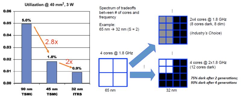
The need to remain within certain limits of power consumption led to the appearance of a restriction called Utilization Wall, according to which with each new process technology and in the absence of radical technological changes, the fraction of the crystal area involved in active work (literally, where transistors can switch) decreases exponentially. Moreover, this area is measured in units or even fractions of percent. [6] The remaining large part of the crystal, which is not currently involved in the work, was called “dark” silicon (“Dark” Silicon).
')
Utilization wall
As a result, developers of microprocessors must be sure that at any moment of operation most of the crystal is “dark” or “dull” silicon — idle or operating at a significantly lower clock frequency.
Michael Taylor in his article “Is Dark Silicon Useful? Harnessing the Dark Horse Apocalypse [4] mentions four "horsemen of the Apocalypse" - four main approaches that allow microelectronics to flourish in the era of "dark" silicon. These approaches: the use of new technological achievements, parallelization for energy efficiency, specialization and energy management. In addition, system level optimization plays an important role. About these approaches and will be discussed further.
"The Deus Ex Machina Horseman" or the progress of the technological process.
“MOSFETs are the fundamental problem. “
We can switch to FinFets, Trigate, High-K,
nanotubes, 3D, for one-time improvements,
but none are sustainable solutions across
process generations.
Of all the four horsemen of the silicon apocalypse, this is by far the most unpredictable. In the literature or theater, Deus Ex Machina refers to a plot in which the main characters seem to be completely doomed, but then something completely unexpected and unpredictable comes from nowhere to save the situation.
In the case of dark silicon, Deus Ex Machina could be a scientific breakthrough in semiconductor technology. However, such breakthroughs should be sufficiently fundamental. And, most likely, in the near future, such a breakthrough will require the use of transistors other than the traditional MOSFET technology. The reason is that leakage currents are determined by fundamental physical principles. Although innovations such as the invention of FinFET / Tri-Gate transistors or the use of High-K dielectrics, etc., represent significant achievements. But they are rather one-time improvements, rather than scalable changes. [8] I will not dwell on the advantages of the Tri-Gate, since they have been written more than once :)
The development of technologies that can replace the MOSFET has been going on for a long time. Two potential and (at the moment) the most promising candidates: these are TFET transistors and nano-electro-mechanical switches. There are reasons to believe that both of these technologies can provide a reduction in leakage currents by orders of magnitude compared with the solutions currently used, but at the same time, they are still very far from industrial use.
One source of optimism about the existence of breakthrough technologies is performance, energy efficiency and density of the human brain. The brain combines 100 trillion synapses that work while consuming less than 20W and serve as living proof of the possibility of highly parallel and, at the same time, mostly “dark” calculations.
As a result, technological advances are still surprising, there are already a number of interesting alternatives to traditional MOSFET electronics. But to predict when these alternatives will get to industrial use, and even more so, the emergence of new ones is not possible.
"The Shrinking Horseman" and Parallelization for Energy Efficiency
“Area is expensive. Chip designers will
just build smaller chips instead of having
dark silicon in their designs! ”
(if you work on Dark Silicon research, you will hear this a lot ...)
Due to the growth of leakage currents as the technical process is scaled, multi-core microprocessors cannot be further scaled in the same way as the area of a crystal that is occupied by a single core. At the same time, “dark” or “dim” silicon is an exponentially cheaper resource in terms of energy consumption. This forces us to turn to architectural solutions that allow one to “consume” the area of a crystal in order to “acquire” energy efficiency. The example shown in the figure shows how replacing one comparator by two, working in parallel, but at half the frequency, can reduce energy consumption by 2.5 times! [9] In practice, not all nodes can be parallelized to close to ideal manners, but the gain in terms of energy consumption will still be noticeable.

Trade-off area and power consumption
The immediate reaction to this approach from many developers was that “the area of a crystal is an expensive resource, why not just make microprocessors smaller, instead of using“ dark ”silicon?” However, this is the most pessimistic scenario. And although all chips may eventually undergo a reduction in area, this view misses a number of secondary factors that play a decisive role.
First, it is worth saying that “dark” silicon does not mean “empty”, “useless” or “unused” silicon. Even on the best days, CMOS technology, microprocessor and other circuits were full of dark logic, which is used only for some tasks. For example, the block for executing SSE instructions on x86 is not used for irregular calculations, and doubling LLC (the last cache level) gives a gain only for a small number of tasks.
Also noteworthy is the financial side of reducing the crystal area . There are some truths in making smaller crystals more profitable. In the end, microprocessor developers spend a lot of effort trying to get into an affordable budget for the occupied area. Smaller processor chips are linear (or even more) cheaper. In addition, for them, the higher yield indicators during production. But exponentially smaller processors will not be exponentially cheaper because of the costs of development, production of lithographic masks, packaging, etc. And these costs must also be somehow depreciated, which will lead to an increase in the cost per unit area of silicon. That, in turn, will make the transition to a new process technology financially less attractive and will lead to the unhappy economic end of Moore's law. There are also a number of other reasons, based on the laws of a competitive economy, explaining why area reduction is an extremely unlikely scenario, but I will not go into details that are not too interesting for the technical readership.
Well, it is impossible not to mention the problems associated with the enclosure and dissipation of heat that occur when reducing the area of the crystal. An important consequence of the exponential reduction in area is the exponential increase in specific power consumption. Recent studies in the analysis of thermal characteristics of multi-core processor chips [10] showed that the peak hot-spot temperature (hotspot) can be modeled as Tmax = TDP * (Rconv + k / A). Where TDP is a value indicating which thermal power is allocated to the processor cooling system, Rconv is the radiator characteristic (less is better), k is the collective characteristic of the microprocessor properties, and A is the footprint. With an exponential decrease in area, the second term becomes dominant and leads to an exponential increase in temperature. The need to protect the processor from overheating will require sacrificing part of its performance.
In addition, area reduction also presents a range of practical engineering issues. For example, a vertical connection of silicon wafers, using technologies like Die Stacking, requires contact pads and slots in silicon (TSVs), the size of which cannot be reduced just as easily. In addition, the I / O connection areas also do not scale with the speed of Moore's law.

3D integration and TSV in pictures :)
As a result: the area of microprocessors will most likely not decrease further (and, if it is, it will be very slow). But if earlier the additional transistors brought by each new generation of the technical process were used to increase productivity (approximately 1.4 times per generation), now they are used to reduce power consumption (approximately 40% per generation)
Continued .
Sources
- Gordon Moore (1965). "Cramming more components onto integrated circuits"
- Mark Bohr, Intel, 2011
- Shekhar Borkar, Intel, 2010
- Mark Bohr, (2007) “A 30 Year Retrospective on Dennard's MOSFET Scaling Paper”
- Fred Pollack, (1999) “New Microarchitecture Challenges in the CMC Process Technologies for CMP Process,” keynote at Micro
- Ganesh Venkatesh et al, (2010) “Conservation Cores: Reducing the Energy of Mature Computations”, ASPLOS 2010
- Michael Taylor, (2012) “Is Dark Silicon Useful? Harnessing the Dark Horse Apocalypse of the Coming Dark Horse, DAC 2012
- Ian Young, Intel, 2012
- Anantha Chandrakasan et al, (1992) “Low-Power CMOS Digital Design”
- W. Huang et al, (2008) "Many-core design from a thermal perspective." DAC 2008.
Source: https://habr.com/ru/post/158223/
All Articles