Reverse Engineering Topology Chips
This post was inspired by the questions that were asked in the topic. How to "open" the microcircuit and what is inside it?
Reversing engineering microcircuits in their topology has been used and is being used not only in the former Soviet Union, but also in the USA, Europe and China. It is used to this day. "Why reinvent the wheel?" It is to recreate the electrical circuit of the chip in its topology. It can be either CMOS or bipolar technology. But only one circuitry for recreating the chip is not suitable. We must learn to model it. Understand how it all works entirely.
In Russia, reversing engineering complex US civilian chips (yes, everybody feels comfortable), the USA is glad to get our unique military chips (yes, and there are a lot of such), China simply copies everything that can only be reached . Just in this way, the development of a fairly complex, necessary for the customer, the chip is accelerated several times. When there is an idea of what is needed from the chip, it remains to find a close foreign analogue, restore it and redo it to fit your needs. It is also possible to make a microcircuit with a radiation-resistant (this is already laid in the technological route of manufacture).
In principle, one person can successfully reversing a chip with topological standards up to 0.5 microns and the number of transistors on a chip up to 5 thousand pieces in 3 months (including disassembling how all this miracle works).
')
The reconstruction of the electrical circuit is carried out by studying and comparing the images of crystals at different strained metallization layers (usually, when the parameters of transistors are obvious). Usually used up to 3 layers of plating. This can be as aluminum, each layer of which is separated by a dielectric (silicon dioxide), and polysilicon, as well as combinations of several types of metallization. If the parameters of the transistors are not obvious, then it will be necessary to study the cross-section of the crystal to understand the structure of the transistor.
I will give an example of the restoration of the electrical circuit of a small piece of crystal chip half-bridge driver, made using CMOS 1 micron technology.
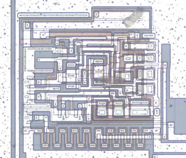
Topology before aluminum etching (i.e., we have 2nd wiring layer).
Topology after aluminum etching (we have the 1st layer of wiring - polysilicon).
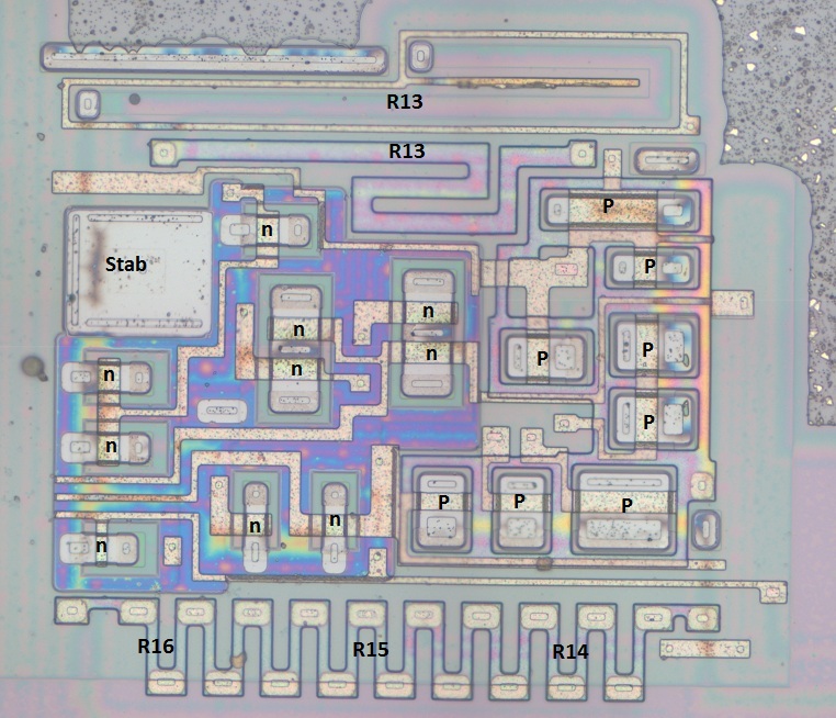
Working with this topology, we find out where the p- and n-type transistors, the resistors material (to determine the resistance), and see the Zener diode. After the restoration of the electrical circuit, we have the following:
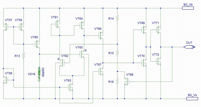
Next, we analyze how this piece of the circuit works and we understand that this element is protection against undervoltage. Quite a smart schema. And very simple to restore and decrypt.
With a good microscope, you can restore almost everything. It is difficult, of course, if there is a “copy protection” - tricks of developers. The main thing then is to analyze and understand how the circuit works.
Thanks for attention! I am pleased to answer your questions!
Reversing engineering microcircuits in their topology has been used and is being used not only in the former Soviet Union, but also in the USA, Europe and China. It is used to this day. "Why reinvent the wheel?" It is to recreate the electrical circuit of the chip in its topology. It can be either CMOS or bipolar technology. But only one circuitry for recreating the chip is not suitable. We must learn to model it. Understand how it all works entirely.
In Russia, reversing engineering complex US civilian chips (yes, everybody feels comfortable), the USA is glad to get our unique military chips (yes, and there are a lot of such), China simply copies everything that can only be reached . Just in this way, the development of a fairly complex, necessary for the customer, the chip is accelerated several times. When there is an idea of what is needed from the chip, it remains to find a close foreign analogue, restore it and redo it to fit your needs. It is also possible to make a microcircuit with a radiation-resistant (this is already laid in the technological route of manufacture).
In principle, one person can successfully reversing a chip with topological standards up to 0.5 microns and the number of transistors on a chip up to 5 thousand pieces in 3 months (including disassembling how all this miracle works).
')
The reconstruction of the electrical circuit is carried out by studying and comparing the images of crystals at different strained metallization layers (usually, when the parameters of transistors are obvious). Usually used up to 3 layers of plating. This can be as aluminum, each layer of which is separated by a dielectric (silicon dioxide), and polysilicon, as well as combinations of several types of metallization. If the parameters of the transistors are not obvious, then it will be necessary to study the cross-section of the crystal to understand the structure of the transistor.
I will give an example of the restoration of the electrical circuit of a small piece of crystal chip half-bridge driver, made using CMOS 1 micron technology.
Topology before aluminum etching (i.e., we have 2nd wiring layer).
Topology after aluminum etching (we have the 1st layer of wiring - polysilicon).
Working with this topology, we find out where the p- and n-type transistors, the resistors material (to determine the resistance), and see the Zener diode. After the restoration of the electrical circuit, we have the following:
Next, we analyze how this piece of the circuit works and we understand that this element is protection against undervoltage. Quite a smart schema. And very simple to restore and decrypt.
With a good microscope, you can restore almost everything. It is difficult, of course, if there is a “copy protection” - tricks of developers. The main thing then is to analyze and understand how the circuit works.
Thanks for attention! I am pleased to answer your questions!
Source: https://habr.com/ru/post/158085/
All Articles