Pictures from printed circuit boards
The concept of making a gift from the boom.
Sokro is coming New Year, St. Valentine's Day, the eighth of March. Yes, a lot of things are coming, and now I want to prepare a sleigh in the summer, a cart in the winter, in general, thoroughly prepare for these festive events and please our second half with something unusual. In my opinion, the most invaluable gift is a gift that is made with your own hands. From here we will dance.
I'm not sure that this idea did not occur to anyone, but fluent googling did not give me any results either in English or in Russian.
')
I spend most of my life doing electronics, programming, and microcontrollers. I was not able to interest any woman, even the most evil engineers, in this hobby. By this, it is necessary for them to at least need to make such a gift so that they understand that in spite of the love of electronics, we love them much more.
For this, I thought to make some memorable electronic device that will remind her of the wonderful moments spent together. Usually a memorable moment is already recorded in the photo ! It remains only to combine photography and electronics.
Imagine a picture: a photograph in a printed circuit board, how you sit in a cafe, and candles are lit by LEDs. This craft is on her desk, and the craft is made by your hands. Hi-tech romance!
Also this technology can be useful for PCB distributors (I send my greetings to colleagues from work) for placing my picture in a printed circuit board (such as a signature).
Speaking in a simpler language, I decided to try to transfer any image to textolite.
Below I will tell you how I did it and what I did.
As we all understand, even a black and white photo has transitions from white to black, called gray. And in the PCB, we have only two colors: the color of copper and the color of PCB. Let's say that copper will be light and textolite black. Although these are all conventions: if you take white textolite and oxidize copper, then everything will be the opposite. How do we make shades of gray in copper?
The idea is simple as everything is ingenious - the technology of placing pictures in a newspaper. The essence is such that the size of the point is determined by the darkness or illumination of the area. Up close it looks awful, but moving away turns out a normal picture.
For the first time I learned about this technology in my childhood, by reading entertaining physics. There was a picture, which at first glance seemed a strange set of points, but at a distance it turned into a woman's eye.

Illustration for “Entertaining Physics”
In order for you not to change the page size, here is a small copy of this image.

In the distance
Perhaps you have already become clear where I am. A photo is taken, transformed into such a sieve, then with the help of LUT or photoresist it is applied to the board and etched.
For all this, you need not a lot, by points:
1. Straight arms growing from the right place.
2. Procurement of PCB.
3. Laser printer.
4. Self-bonding.
5. Hydrogen peroxide, citric acid, salt (cooking).
The most difficult thing for this article was to find a suitable photo. Photos of the models did not take due to copyright issues. Photos from the personal photo archive were either sad or not for a wide range. As a result, for the sample I decided to just shoot one of my favorite tools: mini-disks.
Vices
After that, they must be specially processed. Since I only use linux, I have a warm tube gimp at my disposal.
I did not do it on purpose, no photo processing (highlighting, stretching the contrast, etc.). Looking ahead I will say that I paid for it and the resulting picture was not clear.
So, open the image in gimp, then bleach it.

Bleaching
Then begins the most interesting magic , which turns the usual picture into something that allows you to reproduce it, so to speak, in the gland. Choose “Distortion -> Newsprint”

Magic
After that, we start playing with the parameters. In the section “Divide by:” the checkbox must be checked on CMYK. Experienced way should choose the size of the cell. In the “Black” tab, I personally made the “Slot-function” a line. This is a matter of taste for everyone, but I wanted to try this.

Adjust distortion parameters
Click OK, and we get the following result:

The resulting image
Immediately visible low contrast. But I decided to try, how can we get such less vivid pictures in the gland. See the worst option, so to speak, and continued his experiments. Now it's time to tell how to transfer the resulting drawing to the board.
To transfer the picture, I used the traditional, long-run Laser Ironing Technology (aka LUT). Rather, to remind how it is done, rather than to teach again, I will tell you a few words about it.
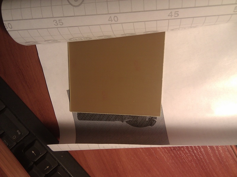
In order to know exactly the size of the future workpiece, I used one simple cheat known from school: placing a picture in a text editor, with the right size. Having opened Writer (an analogue of MS Word in Linux), I set the size of the fields so that the length of the picture horizontally was exactly 10 cm. For this, there is a very convenient ticker at the top of the page. By inserting a picture, you can see that the vertical length is 8 cm.
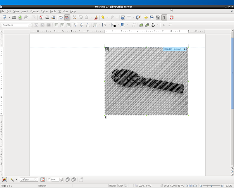
Set clear boundaries
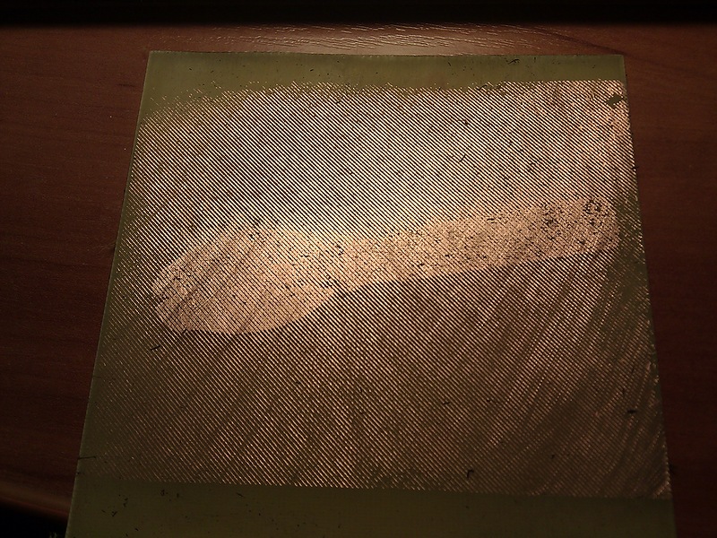
After that, we cut out a rectangle from PCB with the same parameters, skin it and degrease it with isopropanol or with any convenient solvent.

Skins and degrease
You can pay attention to the picture in the top, that as a substrate I use a piece of paper with a test print of the future picture. Having looked at him, I decided to take exactly the lines, and also to increase their stride and thickness.
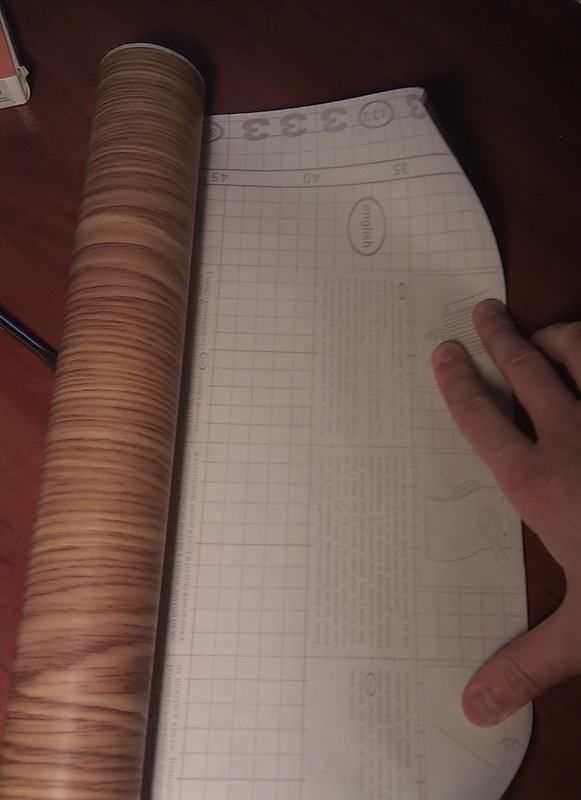
To transfer the image to the PCB, I use a substrate for self-adhesive wallpaper. Unlike magazine paper, there is a million times less gemmoroy and there is no need to soak it. There is a roll of 10 meters of only 250 rubles, and it lasts very long.
On the reverse side, the cells are usually carefully drawn. We attach a sheet of A4, and note which cells it corresponds to.
Markup
You shouldn't be lazy and do a “long A4” (do not cut off the tail), my printer was offended by this and decided that he chewed on the paper that it did not come out for so long.
Cut, tear off the sticker and print on the side that had the sticker on it.

Result (Half Life 2 is not remembered?)
We apply the preparation with copper to the drawing, wrap the textolite in paper, and begin to iron the drawing from the back side.
Wrapping up
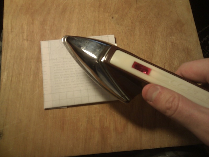
and iron
I usually iron through the blank paper, but then I decided to stroke the paper I had printed on. As a result, the paper stuck to the workpiece, tore the paper with a pattern and everything was rejected. I had to start all over again.
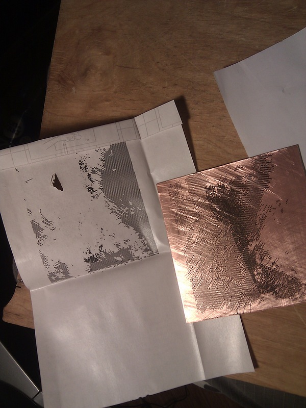
Marriage
Marriage in such matters is a normal phenomenon, so we repeat all the iterations from the beginning. After that, carefully remove the paper from the workpiece and we see the following picture:
Transferred drawing
In connection with the drawbacks of ferric chloride:
- incredibly dirty;
- it is very difficult to wash;
- soils clothes once and for all;
- it is difficult to wash the bath and toilet;
- you need to go to the other end of the city to buy it;
I decided for myself to discover a new way of etching printed circuit boards, described here radiokot.ru/lab/hardwork/62 as the most effective. It requires only three components, which are located in pharmacies and convenience stores:
- lemon acid;
- hydrogen peroxide;
- ordinary table salt.
The etching proportions are taken from the site (I quote): 30 g of citric acid and 5 g of salt are dissolved in 100 ml of pharmacy 3% hydrogen peroxide. This solution should be enough to pickle 100 cm2 of copper, 35 microns thick.
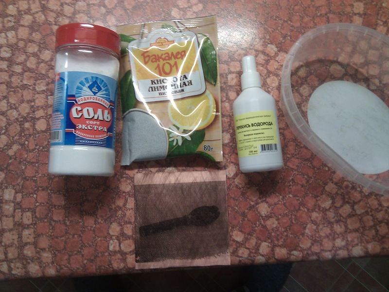
Everything is ready for pickling
Since I did not have dimensional scales, everything interfered with my eyes, trying to at least somehow keep the proportions. In the process of etching, hydroxide began to fall out, and I added more citric acid. Then it became less bubbles, added peroxide. Also spiked salt. Anything is possible with impatience. Everything was poisoned for about two hours. I suppose that this is due to cold peroxide, and it is not my desire to heat it up somehow (it is said that the solution boils, although I personally had a solution that remained cold). Plus, this time I hounded in the pot, without using my wonderful bulbulator , about which I wrote here: habrahabr.ru/post/109869 . And all because he is busy with ferric chloride. It is necessary to make a new bulbulator especially for the new technology.
After etching, a beautiful blue solution is obtained, which, unfortunately, I guessed to take a picture, after I poured it into the toilet. By this, take my word for it, that it is beautiful :).
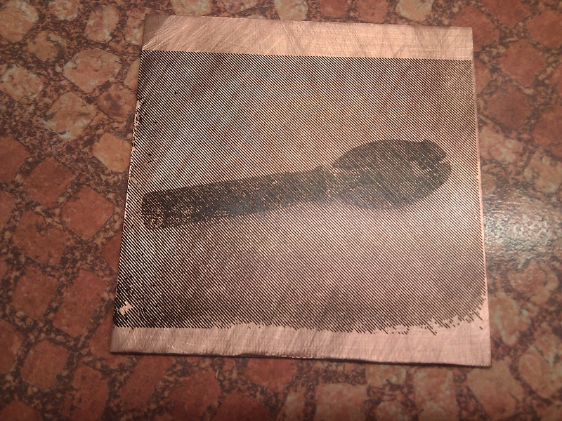
And finally, we can see the result. I will say right away, initially he did not impress me :(.
Etched board
It may seem that there is some hodgepodge and blot on the form of minitisks on the board. But in fact it is not, everything becomes clear, looking at the light

To the skylight
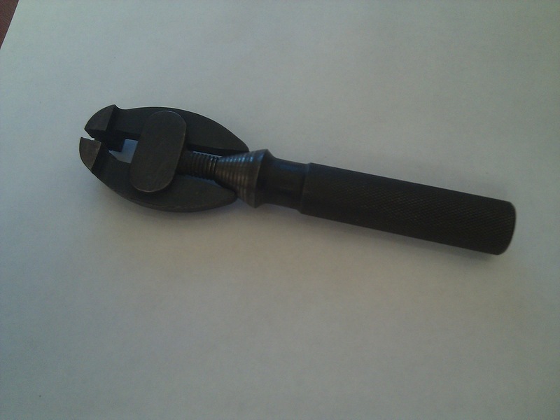
All the details of the minisc are visible to the light, and so that you do not flip to the top, I will bring the original photo again for comparison.

Original photo (reflected horizontally)
Considering the original quality of the photo, it turned out just amazingly, even with low brightness and contrast! All details are visible. Those. technology works!
The technology turned out to be working, and not just working, but a bomb! Perhaps the result for you is not too impressive, but this is only a sample of the pen, which may allow these experiments to develop further.
Even a completely horrible picture got corrupted and turned out. For even better results, use higher-contrast photos. And also expose them to additional processing. It is better to make the background white, or uniform and light.
The lack of technology lies in the low contrast of copper relative to PCB. Solved in several ways. First, you can take a darker textolite. Secondly, you can chemically stain copper. For example, copper darkens in the light, and this picture, if left in the sun for a week, gains enough darkness. I think there are easier ways to oxidize copper, Google to help. However, note that in order to maintain the original shine, I recommend to cover the board with varnish to avoid oxidation.
For use in PCB layout, you must port the processed image into your CAD program in which you deploy PCBs. For P-CAD, this is a very non-trivial and non-obvious path.
The next step will be the introduction of the electrical circuit in the PCB. For example, in order to light and extinguish the stars or the eyes of your beloved at the sight of you :).
I thank my HTC HD2 , peredito on Android for the wonderful pictures and convenient loading them on fotki.yandex.ru
Remember: the best thanks to the author for the post is a comment left.
Sokro is coming New Year, St. Valentine's Day, the eighth of March. Yes, a lot of things are coming, and now I want to prepare a sleigh in the summer, a cart in the winter, in general, thoroughly prepare for these festive events and please our second half with something unusual. In my opinion, the most invaluable gift is a gift that is made with your own hands. From here we will dance.
I'm not sure that this idea did not occur to anyone, but fluent googling did not give me any results either in English or in Russian.
')
Idea
I spend most of my life doing electronics, programming, and microcontrollers. I was not able to interest any woman, even the most evil engineers, in this hobby. By this, it is necessary for them to at least need to make such a gift so that they understand that in spite of the love of electronics, we love them much more.
For this, I thought to make some memorable electronic device that will remind her of the wonderful moments spent together. Usually a memorable moment is already recorded in the photo ! It remains only to combine photography and electronics.
Imagine a picture: a photograph in a printed circuit board, how you sit in a cafe, and candles are lit by LEDs. This craft is on her desk, and the craft is made by your hands. Hi-tech romance!
Also this technology can be useful for PCB distributors (I send my greetings to colleagues from work) for placing my picture in a printed circuit board (such as a signature).
Speaking in a simpler language, I decided to try to transfer any image to textolite.
Below I will tell you how I did it and what I did.
A few words about technology
As we all understand, even a black and white photo has transitions from white to black, called gray. And in the PCB, we have only two colors: the color of copper and the color of PCB. Let's say that copper will be light and textolite black. Although these are all conventions: if you take white textolite and oxidize copper, then everything will be the opposite. How do we make shades of gray in copper?
The idea is simple as everything is ingenious - the technology of placing pictures in a newspaper. The essence is such that the size of the point is determined by the darkness or illumination of the area. Up close it looks awful, but moving away turns out a normal picture.
For the first time I learned about this technology in my childhood, by reading entertaining physics. There was a picture, which at first glance seemed a strange set of points, but at a distance it turned into a woman's eye.
Illustration for “Entertaining Physics”
In order for you not to change the page size, here is a small copy of this image.
In the distance
Perhaps you have already become clear where I am. A photo is taken, transformed into such a sieve, then with the help of LUT or photoresist it is applied to the board and etched.
What do we need?
For all this, you need not a lot, by points:
1. Straight arms growing from the right place.
2. Procurement of PCB.
3. Laser printer.
4. Self-bonding.
5. Hydrogen peroxide, citric acid, salt (cooking).
Image preparation
The most difficult thing for this article was to find a suitable photo. Photos of the models did not take due to copyright issues. Photos from the personal photo archive were either sad or not for a wide range. As a result, for the sample I decided to just shoot one of my favorite tools: mini-disks.
Vices
After that, they must be specially processed. Since I only use linux, I have a warm tube gimp at my disposal.
I did not do it on purpose, no photo processing (highlighting, stretching the contrast, etc.). Looking ahead I will say that I paid for it and the resulting picture was not clear.
So, open the image in gimp, then bleach it.
Bleaching
Then begins the most interesting magic , which turns the usual picture into something that allows you to reproduce it, so to speak, in the gland. Choose “Distortion -> Newsprint”
Magic
After that, we start playing with the parameters. In the section “Divide by:” the checkbox must be checked on CMYK. Experienced way should choose the size of the cell. In the “Black” tab, I personally made the “Slot-function” a line. This is a matter of taste for everyone, but I wanted to try this.
Adjust distortion parameters
Click OK, and we get the following result:
The resulting image
Immediately visible low contrast. But I decided to try, how can we get such less vivid pictures in the gland. See the worst option, so to speak, and continued his experiments. Now it's time to tell how to transfer the resulting drawing to the board.
We transfer the image to the board
To transfer the picture, I used the traditional, long-run Laser Ironing Technology (aka LUT). Rather, to remind how it is done, rather than to teach again, I will tell you a few words about it.
In order to know exactly the size of the future workpiece, I used one simple cheat known from school: placing a picture in a text editor, with the right size. Having opened Writer (an analogue of MS Word in Linux), I set the size of the fields so that the length of the picture horizontally was exactly 10 cm. For this, there is a very convenient ticker at the top of the page. By inserting a picture, you can see that the vertical length is 8 cm.
Set clear boundaries
After that, we cut out a rectangle from PCB with the same parameters, skin it and degrease it with isopropanol or with any convenient solvent.
Skins and degrease
You can pay attention to the picture in the top, that as a substrate I use a piece of paper with a test print of the future picture. Having looked at him, I decided to take exactly the lines, and also to increase their stride and thickness.
To transfer the image to the PCB, I use a substrate for self-adhesive wallpaper. Unlike magazine paper, there is a million times less gemmoroy and there is no need to soak it. There is a roll of 10 meters of only 250 rubles, and it lasts very long.
On the reverse side, the cells are usually carefully drawn. We attach a sheet of A4, and note which cells it corresponds to.
Markup
You shouldn't be lazy and do a “long A4” (do not cut off the tail), my printer was offended by this and decided that he chewed on the paper that it did not come out for so long.
Cut, tear off the sticker and print on the side that had the sticker on it.
Result (Half Life 2 is not remembered?)
We apply the preparation with copper to the drawing, wrap the textolite in paper, and begin to iron the drawing from the back side.
Wrapping up
and iron
I usually iron through the blank paper, but then I decided to stroke the paper I had printed on. As a result, the paper stuck to the workpiece, tore the paper with a pattern and everything was rejected. I had to start all over again.
Marriage
Marriage in such matters is a normal phenomenon, so we repeat all the iterations from the beginning. After that, carefully remove the paper from the workpiece and we see the following picture:
Transferred drawing
We grass
In connection with the drawbacks of ferric chloride:
- incredibly dirty;
- it is very difficult to wash;
- soils clothes once and for all;
- it is difficult to wash the bath and toilet;
- you need to go to the other end of the city to buy it;
I decided for myself to discover a new way of etching printed circuit boards, described here radiokot.ru/lab/hardwork/62 as the most effective. It requires only three components, which are located in pharmacies and convenience stores:
- lemon acid;
- hydrogen peroxide;
- ordinary table salt.
The etching proportions are taken from the site (I quote): 30 g of citric acid and 5 g of salt are dissolved in 100 ml of pharmacy 3% hydrogen peroxide. This solution should be enough to pickle 100 cm2 of copper, 35 microns thick.
Everything is ready for pickling
Since I did not have dimensional scales, everything interfered with my eyes, trying to at least somehow keep the proportions. In the process of etching, hydroxide began to fall out, and I added more citric acid. Then it became less bubbles, added peroxide. Also spiked salt. Anything is possible with impatience. Everything was poisoned for about two hours. I suppose that this is due to cold peroxide, and it is not my desire to heat it up somehow (it is said that the solution boils, although I personally had a solution that remained cold). Plus, this time I hounded in the pot, without using my wonderful bulbulator , about which I wrote here: habrahabr.ru/post/109869 . And all because he is busy with ferric chloride. It is necessary to make a new bulbulator especially for the new technology.
Result
After etching, a beautiful blue solution is obtained, which, unfortunately, I guessed to take a picture, after I poured it into the toilet. By this, take my word for it, that it is beautiful :).
And finally, we can see the result. I will say right away, initially he did not impress me :(.
Etched board
It may seem that there is some hodgepodge and blot on the form of minitisks on the board. But in fact it is not, everything becomes clear, looking at the light
To the skylight
All the details of the minisc are visible to the light, and so that you do not flip to the top, I will bring the original photo again for comparison.
Original photo (reflected horizontally)
Considering the original quality of the photo, it turned out just amazingly, even with low brightness and contrast! All details are visible. Those. technology works!
Summarizing
The technology turned out to be working, and not just working, but a bomb! Perhaps the result for you is not too impressive, but this is only a sample of the pen, which may allow these experiments to develop further.
Even a completely horrible picture got corrupted and turned out. For even better results, use higher-contrast photos. And also expose them to additional processing. It is better to make the background white, or uniform and light.
The lack of technology lies in the low contrast of copper relative to PCB. Solved in several ways. First, you can take a darker textolite. Secondly, you can chemically stain copper. For example, copper darkens in the light, and this picture, if left in the sun for a week, gains enough darkness. I think there are easier ways to oxidize copper, Google to help. However, note that in order to maintain the original shine, I recommend to cover the board with varnish to avoid oxidation.
For use in PCB layout, you must port the processed image into your CAD program in which you deploy PCBs. For P-CAD, this is a very non-trivial and non-obvious path.
The next step will be the introduction of the electrical circuit in the PCB. For example, in order to light and extinguish the stars or the eyes of your beloved at the sight of you :).
I thank my HTC HD2 , peredito on Android for the wonderful pictures and convenient loading them on fotki.yandex.ru
Remember: the best thanks to the author for the post is a comment left.
Source: https://habr.com/ru/post/157465/
All Articles