From programming to hardware or “Why does it not work?”.
Hi Habr. In recent years, digital electronics has become increasingly popular among programmers, new platforms are emerging, allowing various devices to be assembled without any special knowledge in electronics. I myself began to study analog electronics, and later - digital programming. Many - on the contrary - at first programming, and then trying to do iron, while the knowledge of electronics is almost zero and people don’t know / don’t understand things that are elementary for the old electronics electronics engineer. In this article I will try to touch on the most important moments in my opinion, both in terms of circuit design and layout of boards. I hope my advice will help to pass some rakes.
Chip Inputs
Let's look a little inside the microcircuits and see how their parts are arranged. The overwhelming majority of modern digital microcircuits are made using CMOS technology. The base element is a field-effect transistor with an induced channel of p or n type. Combining them according to the following scheme - we get an inverter, when high voltage is applied to the inputs - the resistance of the n channel transistor is small and p of the channel transistor is large, the lower transistor connects the output to ground, but on the contrary - feed a low level - the resistance will be small for p channel transistor - and it connects the output to high voltage.
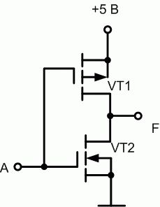
Here lies, at first glance, an inconspicuous thing - and what will happen if the transistors are open at the same time?
That's right - a short circuit between the power supply and the ground - and that’s what will fail faster - the channel of one of the transistors or the power supply circuit that cannot provide such a current. And this may very well be the case. The point here is that for transistors there are voltage ranges on the gate within which we believe that the resistance of the transistor is small or large. Depending on the transistors, they are different - let's say, up to 0.6V, we believe that one transistor is guaranteed to be closed, and the other is open, and above 1.8V, we believe the opposite. The range between these voltages is PROHIBITED in digital electronics, because one transistor can already be opened, and the second is not yet closed. To provide such a condition is quite simple - just leave the unused input of the chip to hang in the air - in this case there can be any voltage. therefore
Tip number 1: always pull up unused chip inputs to any logic level of the circuit. Then there will be less huge eyes and exclamations “Static burned out! You need to wear anti-static bracelets. ”- We need to make the schemes correctly, then they will not burn themselves. Always make sure that the logic level at the inputs is clearly defined at any time during the operation of the circuit. Failure to comply with this condition is fraught with not only errors in the operation of the device, but also its failure. And although the inputs are usually equipped with protective diodes that protect against overvoltage and set the voltage at the gate - you should not hope for them. In addition, chaotically switching elements inside the chip increase its power consumption, which can be critical in battery-powered systems
Chip Outputs
In addition to the inputs, the microcircuit also has outputs - depending on what voltage we apply to the output stage — one or the other transistor opens, through which the current flows, it either flows out or flows into the microchip to get the voltage (because we measure ) current must be passed through the resistance. This resistance will determine the current flowing through the chip output, if we load the output to the high-impedance input 10 MΩ, at a supply voltage of 5 V - a current of 0.5 μA will flow through the controller output. The channel of the transistor has a limitation on the current flowing through it - as a rule, this is reflected in datasheets. The resistance on which the output of the chip is loaded should not be less than permissible. Let's say - if the maximum output current is 10 mA, and the supply voltage is 5V, then the minimum load resistance will be 0.5 kΩ or 500 Ohm, if it is less, it will burn.

Tip number 2:
Connect the output connectors through the pass-through resistors ~ 1 kOhm, because by definition you can connect anything to the output connectors, the pass-through resistor will protect the circuit from curved hands (perhaps even its own). Inside the circuit - if you are sure that the output will always be loaded onto the high-impedance input - you can do without them. All this of course holds true if the output signal is voltage, if current is required at the output — you can configure the outputs in open collector mode, or use an additional external transistor to control the load.
')
Inductance
Inductance is some inertia of the place where current flows - I really like the plumbing analogy here - inductance is a massive turbine that, when pressure is applied, gradually unwinds, then less and less resists the pressure of water, eventually ceases to resist at all, and if you remove pressure, the turbine continues to push water until it stops. In general, at the very beginning of the pressure does the work on the promotion of the turbine, which stores energy in itself. In the case of a current - the same voltage here is the same pressure in the plumbing - we are trying to move the electrons from the place, applying some voltage, but nature is so arranged that some of the energy must be stored in the electromagnetic field - how much - is determined by the geometry of the circuit ( turbine geometry).
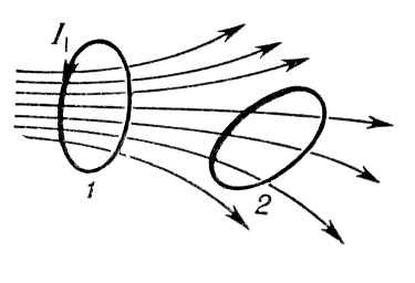
Always remember what you were taught in school - the current flows through the ring! And the area of this ring with current, as well as the thickness of the conductor determine the inductance of the circuit - how much energy will be stored in a magnetic field. This magnetic field can affect other conductors - this phenomenon is used in transformers. Any 2 circuits with current have mutual induction and one will influence the other. Secondly, high inductance limits the speed of the circuit, in addition inductances with parasitic capacitances can form resonant circuits and the circuit can work unpredictably ... But first things first - I will tell you about some effects associated with inductance in digital technology
Lead inductance, double frequency operation
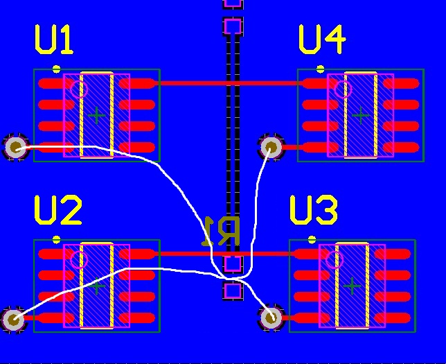
Any piece of conductor through which the current flows has its own inductance, including the legs of the microcircuit. Let's see what it can affect. Consider the following scheme - all that in the yellow square is a chip of the chip, the internal power lines are connected to the external ones through the inductance of the legs.

Suppose a high logic level was maintained at the output — a small current flowed through the input impedance of the receiver and the input capacitance was charged, and then the output was switched to a low logic level. The lower transistor opens, the upper one closes, the capacitance C is charged, the resistance R is large, the capacitance will discharge through the lower transistor and the inductance of the earth output - what do we have? After switching the output from 1 to 0, we get a current inrush due to the input capacitance of the receiver, the current passing through the inductance of the earth output causes a self-induction EMF, the internal ground thus jumps relative to the external one by the value of this EMF equal to -LdI / dt, and the derivative sign will first be positive - the current through the inductance increases, and then the negative one - the current drops. We receive impulse noise on the internal tire of the earth - its potential will first jump, and then it will drop by the same amount.
But all internal measuring circuits use the ground potential as a reference! Only he jumps, with other signals on the valves nothing happens. Now imagine that our chip is clocked from an external generator and its outputs are not 1, but 8 - 32 - some kind of memory chip with separate outputs for reading and writing - at the same time we write and read - first we set the data on the inputs that we want to write , then we issue a clock signal - the input data is latched, and the output is set. The clock signal recognition mechanism — differential — internally measures the difference between the voltage at the clock synchronization input and the internal ground. Suppose there is a switching on the clock signal of outputs from the state 0xff to 0x00 - while the voltage of the impulse noise will be 8 times greater than with 1 foot - the internal ground jumps first, and since the difference between the input signal and the internal ground is important - it can jump up to the point that the internal comparator switches to 0, then the earth drops and the comparator switches to 1 again - we get an additional clock immediately after the first one, while the new input data have not yet been set, and the weekend has not yet been taken. Outwardly, this will not manifest in any way - the circuit will simply fail to understand why - everything will be clean on the oscilloscope, but you cannot stick into the chip.
Manufacturers solve this problem by reducing the inductance of the leads, creating leadless housings, which also save space. But all this at the cost of reducing mechanical reliability and mounting complexity. In addition, one of the solutions is to use separate leads for measuring circuits, several ground and power pins are also used - in this way the inductances of the leads are connected in parallel and the total inductance decreases, moreover, it allows to distribute the currents inside the crystal and reduce their influence on each other.
Tip number 3:
If the microcircuit has separate power pins - everyone should have their own connection point to the ground bus or power supply - you do not need to connect them together, and then attach it all to the bus with one bit - this is how you kill the whole idea!
Mutual induction circuits with current guidance
Remember I said that the current flows in a ring? This should always be remembered when you are developing a high-frequency device. At high frequencies, the line resistance begins to play a smaller role, compared to inductance — the RF current does not flow along the path of least resistance, but along the path of the smallest inductance, the current always tends to form a circuit with the lowest inductance — that is, the reverse current tends to flow as close as possible to the track along which the direct current flows - so the area of the circuit will be minimal, respectively, its inductance will be minimal. The smaller the inductance of the line - the higher its speed (the turbine is easier to unwind), besides - the reverse currents of different lines should not flow in the same place - so they have a high mutual inductance - one circuit starts to give noise to another, like in a transformer . In general, all you need to do when wiring a printed circuit board is to allow reverse current to flow under the track.
Here is an example of how not to do it: - a section is in the earthen layer - a reverse current from the upper pair of the receiver - the transmitter is forced to bend around the section - this causes an intersection with another current loop and the area and inductance of the circuit increases
Tip number 4:
Watch the return paths of the signal currents - the current itself seeks to minimize the inductance - you simply should not disturb it. Make sure that the contours intersect as little as possible - this will increase the noise immunity of the circuit.
Tanks
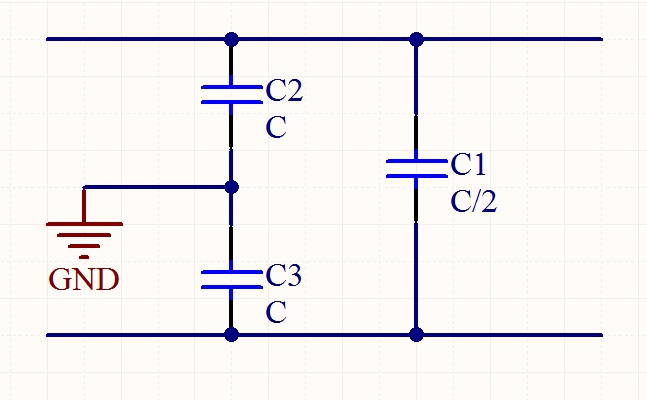
Everywhere, where there are 2 conductive surfaces - there is a capacitance - whether it be wires, conductors on a printed circuit board or legs of microcircuits - sometimes capacitance is good sometimes bad. For example, in the case of operation at double frequency — the large input capacitance of the receiver — is bad, because the amount of charge it receives increases, respectively, the amplitude of the impulse noise. If in the case of inductance - the connection goes through the magnetic field, then in the case of capacitance - electric, the area of conductors and the distance, as well as what is located between them, plays a decisive role. For example, capacitive coupling between conductors in a bus is bad (for example, IDE cable) - it can be minimized by earthing conductor between tracks, then the equivalent circuit will be the following: C is the capacitance between two conductors. - in this case, the effect of mutual capacitance decreases firstly - by 2 times due to the increase in distance, secondly - we have 2 parallel-connected capacitors - one goes to the ground, the second to another conductor - one has an impedance of 1 / iwC, the other 2 / iwC, the alternating current is divided between them in the ratio of 2/1, that is, the presence of an earth conductor between the lines reduces the influence of mutual capacitance by 4 times
If there are 2 earths in the circuit - analog and digital or high current and low current - you need to make sure that the mutual capacity between polygons is minimal - you can achieve this by making one of the polygons a grid. But it is worth warning that reducing the capacity of the landfill is not always beneficial
Blocking capacitors
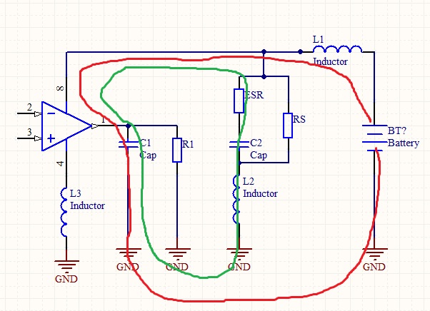
Generally speaking, for an alternating current it does not matter - to flow on the ground or on the power bus - for him they are equal. In the ideal case, the power supply should have zero impedance, but in reality this is not the case, the input wires and power wiring contribute to this. What is bad? Suppose - some kind of chip output has switched from state 0 to state 1 - while the output capacitance must be charged. and where to get electrons for charge? correctly - from the battery, that is, every time we switch we have a pulsed inrush of current in the power circuit - and so every time we switch something inside the chip, but what does the current do when it flows through the inductance of the power circuit? interferes with other such circuits — if there is no low AC impedance between the power supply and ground and the current has no other way than through the battery — the level of crosstalk in the circuit increases. The problem is solved by installing blocking capacitors next to each microcircuit - these are essentially small batteries with low impedance - with the help of them we divide and reduce the circuits of alternating currents of microcircuits. It is worthwhile to dwell a little on capacitors — in the above diagram, L2, C2, ESR, ES is the equivalent circuit of a capacitor — L2 is a series inductance of the leads, C2 is the capacitance itself, ES is the dielectric resistance, ESR is the equivalent series resistance — stick a piece of PCB into the microwave and turn on warm for a few seconds? This is the equivalent series resistance - the fact is that a dielectric is dipoles - essentially 2 balls connected by a spring - it is an oscillatory system that has its own frequency - if you change the external field with a close frequency - the resistance is small, if it is excellent - the system is more difficult to make oscillate - ESR depends on the frequency and has a resonant peak - in the vicinity of this peak the ESR is small - the position of this peak depends on the material of the dielectric - in electrolytic capacitors it is at low frequencies, eramicheskih - on the higher. Thus, in order for a capacitor to have a small impedance, we must ensure the minimum inductance of the terminals and the minimum ESR
Tip number 5:
To reduce crosstalk along the power lines, try to minimize the impedance of the power supply wiring, if possible use polygons for power supply and ground - the capacitive coupling between them helps reduce the impedance.
Since it doesn’t matter for AC — returning along the power line or on the ground — use capacitors so that the return current can flow from layer to layer if necessary. Place blocking capacitors in close proximity to the microcircuits, to minimize crosstalk along the power lines. Use capacitors with different types of dielectrics.
That's all - I hope someone the article was helpful - leave your questions and comments in the comments or in the LAN
Source: https://habr.com/ru/post/156977/
All Articles