Microelectronic industry in Russia (2012)
 With theory (1) (2) finished - it's time to move on to practice. In this article - about which microelectronic plants in Russia (and Belarus) exist and what they can do, as well as about the largest developers of the microchips themselves, and what working results they have achieved.
Under the cut - a dramatic story about plastic electronics, the Russian "humanitarian aid" familiar to many of AMD and Metro tickets.
Well, in addition - a graph showing how the state of Russian microelectronics has changed over the past 22 years compared with the United States and China.
')
Graph of the comparative state of microelectronics
Technological lag figures / benefits are built “optimistically”: for how many years the USA / China has the following technology. For example, since 2012 we have 90nm - the United States has the following technology (65nm) since 2006, respectively 2012-2006 + 1 = 7 years.The blue graph is the USA, the red one is China.
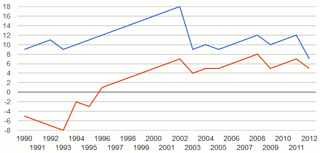
As I wrote in previous articles, in the race to meet the demand for iPhones, money cannot be earned (if you are not a leader), therefore there is nothing dramatic in the current situation as long as the industry can produce critical products (and 90nm is more than enough for industrial and military / space electronics).
But it’s already time for us to stop considering China a technologically backward country: in fact, they have been in microelectronics for many years ahead of us. At the moment, they have launched production of 45nm, and have a license for 32nm.
Microelectronics manufacturing
Sitronics - Micron
Until 2010, Micron worked at near-micron norms, on equipment most of which remained from Soviet times.
In 2006, the technology and equipment for production with standards of 180nm (CMOS + EEPROM) with aluminum metallization on plates with a diameter of 200mm from STMicroelectronics was purchased. Then, on the basis of this equipment, SiGe technologies (necessary for radio frequency applications - GLONASS, radar, etc.) and SOI (for radiation-resistant microcircuits) were developed (or purchased - there is no data here). The production volume is 1500 plates per month.
At the end of 2007, however, they only solemnly cut the ribbon, the first test plates were in 2010. Such an early “ribbon cutting” is exclusively a matter of tax optimization.
There were reports that Micron made RFID chips for subway tickets - but having opened 30 subway tickets in the last six months, he found only NXP chips. The same result came in August 2009 and in the company Chipworks . However, I don’t see any drama here, it’s not for the metro that they bought this production. In Micron itself, my questions on this topic were left unanswered. However, it seems that one person was lucky to see the Micron chip 1.5 years ago.
That's what's now inside each ticket metro: (size - 0.6x0.6 mm)

Then, from the same STMicroelectronics, a 90nm technology with copper metallization was acquired, which requires additional equipment (mainly scanners) with an increase in production capacity up to 3000 plates per month:
ASML PAS 5500 / 750F 248nm / 0.7 120 plates per hour
ASML PAS / 1150C 193nm / 0.75 135 plates per hour (Russia's first scanner at a wavelength of 193nm)
Financing involved Rosnano. In September 2012, they announced the start of sales of 90nm products. Thus, at the moment Sitronics-Micron - has the most modern and versatile semiconductor production in Russia, having spent on it very modest money by world standards.
Micron has a younger brother - VZPP-Micron, in Voronezh - there they make discrete elements, and microcircuits on micron norms.
NIISI RAS
Or as it is called - "Kurchatnik". There is a super-small-scale production, stepper - ASML PAS 5500 / 250 with a resolution of 350nm. Production volumes - read plates per day. Engaged only in military products, of the little known, developed and produced in Kurchatnik - Komdiv-64 .
Integral
For a long time, Belarusian Integral had 800nm technology, but a few years ago they were finally able to launch 350nm production on 200mm plates, with a production volume of 1000 plates per month. There is also a production of “clean” plates with a diameter of 200mm for a 350nm ruler.
On the new line - they seem to be engaged only in military chips, but in the old giant production (150mm / 800nm - 10 thousand pl / mo, 100mm / 1.5µm - 30 thousand pl / mo, 100mm / 2µm - 15 thousand pl / mo) produce discrete components and simple chips for export.
Angstrom ("old")
On the old Angstrom - production with standards of 600 nm on plates with a diameter of 150 mm (8 thousand plates per month) and 100 mm, 1200 nm silicon-on-sapphire / silicon carbide (4 thousand plates per month).
Steppers - Cannon FPA-2000 i1 (wavelength 365nm, NA = 0.52, resolution ~ 0.5um).
Like other domestic factories, civilian products are exported (LED drivers, power management microchips for cell phones, etc.).
Angstrom-T
Angstrom-T has already managed to generate a lot of drama - so dwell on it in more detail. The project is based on the case of an unfinished plant, which remained from Soviet times. The case was built soundly, and met the modern requirements of 130nm technology.
The equipment was purchased by AMD (130nm, copper metallization in 9 layers, 14000 plates per month) taken from the Dresden plant, and the banquet was financed almost entirely by VEB's credit line with a limit of 815 million euros, which is in principle a unique case - microelectronic factories are rarely financed for credit score of more than half. You can also read an article about the construction site in 2010 - habrahabr.ru/post/80142
In 2008, AMD paid for equipment ~ 182.5 million euros, ~ 120 million euros - a license for the technology, ~ 10 million euros - to Meissner & Wurst for the stage A of the plant design. However, the owner of the equipment was not Angstrom-T, but the Cyprus offshore company Runica. The equipment was also not brought to Russia, but left in warehouses in the Netherlands and Dresden, so the VAT was not paid either in Europe or in Russia. You can watch the video shot at that moment - tv.cnews.ru/?video_id=410
Then, suddenly, the financing stopped (the testimony of the parties differed - the crisis was tolly, the loan was overdue), the equipment remained abroad (now it is also necessary to pay for storage in special warehouses and insurance annually). In fact - the minimum possible amount spent to pay AMD was spent - and the project stopped there. By the way, as we remember, AMD just at that time separated its microelectronic production into a separate company (this was completed in March 2009), and the company very quickly succeeded in pushing its outdated equipment at a very good price.
After the cessation of funding, there was no visible progress on the project, only mouse fuss (who is insuring what to whom, change of owners and managers) and interest accumulation on the credit line. In 2012, funding was resumed (however, there were reports of renewed funding earlier), and at the end of October 2012, Angstrom-T was “officially” bought by Leonid Reiman. At the same time, 90nm technology is licensed from IBM, which will require the purchase of additional equipment. Construction has been resumed, and the start of production is now planned for the beginning of 2014. Of course, the transition to the next technology will somewhat compensate for the extra 5 years that the equipment has been in stock.
It should be noted that up to 65nm in this way does not “upgrade” - 65nm usually requires 300mm plates for economic reasons.
Calculate money (very approximately)
Let's take a rough look at what is on the fingers of what the financial future of the project may look like in the most optimistic way:
The initial size of the credit line for the construction and launch of the plant is ~ 815 million euros. Let's forget about the percentages that have already come up since 2008.
For example, IBM is not so greedy, and additional equipment along with a 90nm license will cost only $ 100 million (for comparison, Sitronics for a 90nm license paid 27 million euros, according to the press).
Then the amount to return ~ 815 * 1.29 + 100 = $ 1151 million, the rate of 8.5%
According to the original business plan - the cost of materials, electricity, water and gases for the production of one plate, minus the cost of masks (they are paid by the customer) is $ 408.75. These are our conditionally variable expenses per one plate, we bear them only if we have production.
The annual cost of labor with traditionally low wages:
1098 (state size) * 12 * 30000 = 395.2 million rubles per year.
We assume that we do not need to pay anything more (for example, taxes). These 395.2 million rubles are conditionally fixed expenses, we bear them regardless of how much production the plant has.
Graph of the average cost of finished plates with a diameter of 200mm in the world market:

I think it would be fair to assume that the average cost of the finished plate is 200mm 90nm in 2014 - about the same as 200mm 130nm in 2009. By the way, pay attention to the same price of 350-150nm plates - this is due to the fact that a loan for equipment and construction has been paid for a long time by all market participants, and everyone works at almost the cost price (and labor and materials cost about the same).
Then for the year the plant minus the most basic expenses will receive:
14000 * 12 * 1001 (revenue with maximum load) -395.2 million rubles / 31 (semi-fixed costs) -14000 * 12 * 408.75 (semi-variable expenses on one plate) ~ $ 86.75 million
And only interest on the loan at a rate of 8.5% will be $ 1151 * 0.085 ~ $ 97.8 million
Thus, even in greenhouse conditions, and 100% load - the plant will not be able to pay even interest.
If you write off 50% of the loan - the loan in the same greenhouse conditions will be able to pay for 13 years, but in reality - there will be enough complications (for example, a further reduction in the cost of the plates over time, not full plant utilization, etc.)
How did the project initially receive funding from such perspectives? The business plan included an optimistic estimate of the plate cost of about $ 2000-2500 + some administrative resource (since the project was important for the development of the Russian electronics industry).
Thus, without credit cancellation, nationalization, annihilation of the eurozone, massive multi-year subsidies in any form (at the level of $ 100 million per year) or a nuclear war in Taiwan and South Korea, the plant will not be able to work. But surely Reiman knows more than we, once officially got involved in this business - it remains to wait for 2014-2015 and see what happens.
Other
In addition, there are smaller enterprises with micron-thicker production: Exciton , NPO IT (for space), Voskhod-KRLZ , production of photo masks - PCU PKIF and others.Related production, caught in the news
Plastic logic
The company was engaged in e-ink displays based on "plastic" transistors. The advantages are their flexibility and potential simplicity of manufacturing, but the electrical parameters of plastic transistors are orders of magnitude worse than silicon ones (therefore, no revolution and murder of “outdated” silicon electronics are foreseen).At the end of 2010, Rosnano invested in Plastic Logic subject to the construction of a screen reader plant in Zelenograd.
October 11, 2011 Interfax: RUSNANO increased its share in Plastic Logic to 43.8% from 33.7%At the beginning of 2012, the company suddenly decided that the moment had been lost, and it was no longer profitable to build a plant . The company will now be engaged only in the development and licensing of technology (however, who now needs this licensing, if the market is swamped).
[...] Plastic Logic's valuation has not changed, the invested funds will be fully used for the construction of a plant in Russia, RUSNANO said.
Construction of a plant for the production of non-silicon displays in Zelenograd is scheduled to begin in December of this year. The company will produce about 100 thousand displays per month. [...]
Epic fail.
Crocus Nano Electronics
May 17, 2011 RUSNANO Press Center: RUSNANO and Crocus Technology create MRAM production - for the first time in the world using 90 and 65 nm technologyHowever, this is not a full-fledged 65nm production ($ 300 million is a penny for a full-fledged 65nm production) - they will take ready-made CMOS plates (with transistors and metallization), and apply a layer for magnetoresistive memory. Let's wait for 2013 and see what happens.
RUSNANO and Crocus Technology, a leading developer of magnetoresistive memory, today announced the conclusion of an investment agreement on the creation of the next generation MRAM memory production in Russia. The total amount of the deal is $ 300 million. Under the agreement, RUSNANO and Crocus create Crocus Nano Electronics (CNE), which will build a medium-density and high-density MRAM memory production plant in Russia with design standards of 90 and 65 nm using thermal switching technology (Thermally Assisted Switching - TAS), developed by Crocus.
GS Nanotech
25/09/2012 RIA News: The center for the production of microelectronic components will start working in the autumn near KaliningradIf you look at their site , then it is immediately obvious that the company is engaged only in cutting plates, enclosing and testing microcircuits. Those. At the entrance - ready plates, at the exit - chips. This is undoubtedly an important matter, but “45nm” - there is no side to the enterprise here at all.
The first large-scale enterprise in the Russian Federation for the production of microelectronics components with a topology of 45 nanometers and less, the GS Nanotech Center, located in the Kaliningrad region, will be commissioned at the end of autumn, Alexey Yartsev, the production manager of the center, told reporters.
MAPPER Lithography
Rosnano has invested € 40 million in the technology of maskless lithography. This, in my opinion - the most delicious investment Rosnano. Without mask lithography is a future revolution in small-scale production of microelectronics (goodbye FPGA), and this is especially useful for the production of military microelectronics: now you do not need to order a set of masks for $ 150-500 thousand to produce 10 microchips, or to wait a dozen "neighboring" projects to printed on the same mask and one production technology.
The essence of the MAPPER technology is the electron-resist exposure by an electron beam. This has been done before, but now - the rays are not 1, but 13'260. Thus, one unit will be able to exhibit from 1 to 10 plates per hour, which is quite enough for many small-scale products.
Microelectronics Development
I will note the most interesting, in my opinion, domestic developments, not covered with a veil of secrecy:MCST
MCST-R500S (500 MHz SPARC 2 core)Elbrus-S (500 MHz, own architecture)
MCST-R1000 (1GHz SPARC, 4 cores)
ELBRUS-2S + (500 MHz, 2 Elbrus cores, 4 DSP cores)
Elvis
1288HK1T (MF-01) - 4-channel SDR receiver1892BM5Y - 1.2GFLOP DSP (32-bit)
1892BM10YA - 4 GFLOP DSP (32-bit) with GLONASS support
Milander
1986EV92U / MDR32F9Q2I ARM Cortex-M3 128kb flash / 32kb SRAM, 80MhzK1986BE21U / MDR32F2QI ARM Cortex-M0 128kb flash / 16kb SRAM, 36Mhz
STC Module
1879BM3 - 4 8-bit DACs, 300 MHz, 2 6-bit 600 MHz ADCs, 150 MHz processor core and external memory interfaceNM6406 - 300MHz DSP (2 32-bit MAC per clock)
KM211
K5512BP1F (Quark) - 150MHz 32-bit RISC processor, manufactured in Micron, 180nm eachSummary
In recent years, Russian microelectronics has significantly come to life, both in terms of production (90 and 180 nm on the Micron, 350 nm on the Integral), and development.Now it is already possible to develop and produce absolutely any industrial, military and space products - processors, microcontrollers, power electronics, radiation-resistant microcircuits, circuits for radio communication, GLONASS and radar. But as we remember, development is an expensive pleasure, so it’s impossible to do everything at once.
In microelectronics, there is no “outdated” production, products by any standards have their own market and price. Even Soviet factories are still working for export - producing power chips, discrete elements (power transistors and diodes) and other small things - and we then buy them in motherboards and cell phones under foreign trademarks.
Source: https://habr.com/ru/post/156843/
All Articles