How does microelectronic production work and what should we build a house?
 Many probably wondered more than once why the processors, video cards and motherboards we buy in stores are designed and made anywhere, just not in Russia? Why is it like this, can we only pump oil?
How much does it cost to start the production of microcircuits, and why, if there are 22nm factories, most of the microcircuits around the world are still being made on “outdated” 180nm-500nm equipment?
Answers to these and many other questions under the cut.
')
How does microelectronic production work and how much does it all cost?
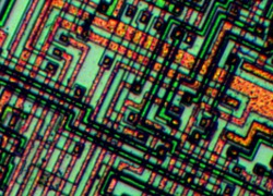
Silicon wafer transistors are drawn using photolithography using devices called steppers or scanners. Stepper - draws a frame (up to 26x33mm) entirely, then moves to a new position. Scanner - simultaneously moves the mask and the plate so that at each moment draw only one narrow “line” in the center of the frame, thus the aberrations of the optical system have less effect on the image.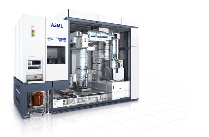
The main characteristics of steppers / scanners are the wavelength of the light at which they work (on i-line mercury lamps - 365nm, then on excimer lasers - 248nm and 193nm), and the numerical aperture of the lens . The shorter the wavelength, and the larger the aperture, the smaller the details can be drawn by the lens in accordance with the diffraction limit:
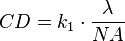
For example, for one of the most advanced ASML NXT 1950i scanners with a wavelength of 193nm and a numerical aperture of 1.35, and k1 = 0.4 (the usual value for photolithography without “tricks”), we obtain a theoretical resolution of 57nm. Using tricks like phase masks, multiple exposures, optical proximity correction, off-axis illumination , light polarization - get minimal elements up to 22nm.
Other parameters of steppers / scanners are performance (how many plates per hour they can process, up to 220 plates), and a combination error (by how many nanometers in pieces does the positioning of the plate relative to a given position miss. On modern scanners it is up to 3-5 nm).
Steppers / scanners print a 4–5 times smaller image of such a mask (a glass plate with a chip pattern, about 15x15 cm in size) in precisely defined places.
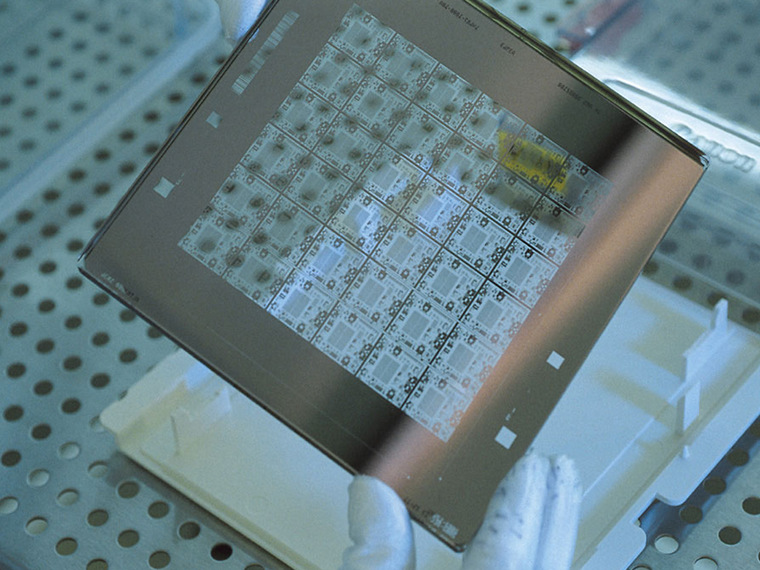
The operation of printing the pattern (with different masks) must be repeated from ~ 10 (for the simplest and oldest chips) to ~ 40 times to form all the necessary layers on the chip (starting from the transistors themselves, and ending with 2-10 layers of metal connections). Between the photolithography operations, the plates undergo various processing - they are heated in the oven to 1100 degrees, poisoned in solutions and plasma. At the exit, the plate remains to be cut into individual crystals, tested and placed in the housing.
The “toughness” of the technology is measured by the size of the minimum element to be drawn (some parts of the transistor, for example, a gate, can be either smaller or larger than this figure — that is, this value is rather relative). It is clear that the smaller the transistors - the faster the chip, and more crystals fit on the plate (but not always need the maximum speed).
Now begins a slow and painful transition to EUV-lithography, with a wavelength of 13.5nm and mirror optics . EUV scanners are more expensive and slower than the usual 193nm, and are just beginning to exceed them at an achievable resolution.
How much is your processor worth doing?
The numbers are rough estimates, they will not be accurate anywhere without the NDA.Software license for one workplace of a chip developer - from $ 20,000 to $ 100,000 a year and higher. Of course, you can steal, but everyone is watching this.
Next - the manufacture of masks. They should not have any damage, and their production is very expensive: from ~ 7'000 $ per set for 1000nm chips for ~ ~ 100'000 for 180nm chips and up to ~ 5'000'000 $ for 32nm chips . But the microcircuit will probably not work the first time, and after finding the mask error, you will have to redo it. In part, this problem can be dealt with by placing test chips from many customers on one set of masks - then everyone will get a little bit of test chips for 1/3–1 / 10 of the price of a full set of masks (this is called Shuttle or MPW - multi project wafer).
Each plate produced costs from $ 100–400 for old technologies at 1000nm, ~ $ 1000 at 180nm and up to ~ $ 5000 for the most modern ones (in addition to nanometers, the complexity of the technology also influences - simple logic is cheaper, flash memory is more expensive, but not many times ). Here it is also important to remember the size of the plates: the most modern production now work with plates with a diameter of 300mm - they are approximately twice the area of plates for 200mm (which are now used in Russia on Micron, Integral and in the foggy future on Angstrom-T), and the last about twice as much even older 150mm. Larger plates make it possible to get chips of lower cost for large orders because The number of body movements for the manufacture of 100 plates is about the same, regardless of diameter (this is one of the reasons for the planned transition of advanced production to plates with a diameter of 450mm in 2018, according to optimistic estimates).
Suppose we want to develop an x86-compatible processor (or any other relatively complex microcircuit), using 28 / 32nm technology that is more or less modern (22nm does exist, but commercial orders are not yet placed - so access to technology is sometimes like love: for money is not for sale). The issue with the cost of patents is omitted, it is generally a very sad topic. Suppose you need 200 mythical person-years for development (if we are doing a modest processor that does not claim to be in the first place).
Software licenses - 50k $ * 100 = $ 5 million (rough estimate, not everyone needs a license).
Salaries of developers - let's say 3k $ * 1.5 (taxes) * 12 * 200 = $ 10.8 million
Test launches in MPW - $ 2 * 1.5 million
Manufacturing masks for mass production $ 2 * 5 million = $ 10 million (2 - because no matter how hard you try, it won't work the first time)
Total - $ 28.8 million
This was what is called Non-recurring engineering (NRE) - one-time costs that do not depend on the volume of production, and the success of the entire event.
If we have a processor with an area of 200mm2, plates using a 32nm technology with a diameter of 300mm cost $ 5000, then from the plate we will get 70690/200 = 350 crystals (estimate from above), of which we will work 300. That is crystal prime cost - $ 16.6, $ 20 after packaging. For how much now such a processor can be sold? $ 50? $ 100? We take taxes and mark-up stores ...
And now the question is - how much do you need to sell such processors to recoup our NRE, interest on loans, taxes, and so on? Million? 5 million? But the main question is whether there are any guarantees that these 5 million processors will be able to be sold, given that competitors do not have to produce anything 5 million more than their already finished product?
Here is such a hellish business it turns out - huge capital expenditures, huge risks and moderate profits at best.
China - solved the problem in its own way, they decided to put computers with their processors and Linux in all schools - and the problem with production volumes was solved ( (1) (2) ).
Thus, the main question when creating microchips is not how and where to produce, but how to develop and to whom then sell millions of the resulting products?
And how much does a plant cost to build?
The cost of a modern plant is approaching $ 5 billion and above . This amount is obtained because the cost of licenses and some other fixed costs do not greatly depend on the volume of production - and it is advantageous to have large productions so that the costs are “smeared” over a large volume of products. And every modern scanner (which actually draws these 22–32nm parts) costs between $ 60–100 million (there may be a couple of dozen of them in a large factory). In principle, 5 billion is not so big money across the country. But naturally, no one will spend 5 billion without a clear plan for the return on investment. And the situation there is this - despite the complexity of the industry, only monopolists work with visible profits (TSMC, Intel, Samsung and a few others), the rest barely make ends meet.
It simply did not fit in my head - how could it be to invest billions and barely barely beat them off? It turned out that everything is simple - around the world microelectronics is the most severely subsidized industry - factories are constantly begging for exemption from taxes, soft loans and dumping (in China they went even further - SMIC builds plants at public expense, and then they “manage” - this is called Reverse Build-Operate-Transfer ). After the appearance of each new technology (45nm, 32nm ...) - the first monopoly plants possessing it and chop the main profit, and those who come 2-5-10 years later than the start - are forced to work practically at cost. As a result, the money here is extremely difficult to earn (without a monopoly and without subsidies).
It seems to have been understood in Russia too - and the projects of large microelectronic plants have so far been postponed, and small productions are being built - in order to lose money, then to lose them a little. And even 3000 plates per month, produced in Micron - it covers the volume of consumption of tickets for the Metro and the defense industry (the subway ticket crystal has a size of 0.6x0.6mm, on a single 200mm plate you get 87'000 tickets in the subway - but about a sad story with tickets I will tell the metro in one of the following articles).
Contrary to popular belief, there are no special restrictions on the sale of equipment for microelectronics to Russia - a presidential moratorium is imposed annually on the Jackson-Vanik amendment in the United States, and you only need to receive a normal export permit. The equipment manufacturers themselves are vitally interested in making more money, and for their part, they are kicking the issuance of permits. But naturally, without money, no one does anything. So for your money - every whim.
But it must be remembered that its plant does not guarantee complete independence of production, and is not cheaper than production abroad: the main cost is technology / licenses and the cost of purchased equipment — and if there is no technology and equipment, and to import everything, then it will be cheaper can not. Many consumables also have to be imported anyway. A separate sore point is the production of masks, only very large factories can have “their” production of masks.
And how many nanometers do you need for happiness?
It seems to many people - well, Intel has 22nm, and we have 90nm - as we hopelessly lagged behind, feed the tractor ... But there is another side to the coin: look at the same motherboard, for example: there are hundreds of semiconductor devices - MOSFETs, drivers, power chips, any auxiliary trifle - almost all of them have enough 1000nm technology. All industrial electronics, and microcircuits for space and the military - in almost 100% of cases, the technology is 180 nm and thicker. Thus, the latest technologies are needed only for central processors (which are very difficult / expensive to do because of the high risks and high threshold for entering the market), and various “asshole” (iPhones and so on). If a war happens suddenly, and Russia loses imports, it will be possible to live without zhopogrek, but without industrial, space, and military electronics — no. Those. in fact, we see that things that are critical for a country are done as much as possible in Russia (or purchased for the future), and we can import at least, as a last resort, as a last resort.There are other factors - the same cost of masks. If we need to make a simple microcircuit, then to make for its manufacture a 32nm mask worth $ 5 million - it can be beneficial if this microcircuit is then produced in tens and hundreds of millions of copies. And if we need only 100'000 microcircuits, it is more profitable to save on masks, and to produce a microcircuit using the most “thick” technology. In addition, there are contact pads on the microcircuit, to which microcircuit pins are connected - there is no way to reduce them, and therefore, if the microcircuit's area is comparable to the area of the pads, then there is no point in making the microcircuit using thinner technology (of course, “thick standards” meet the requirements on speed and power consumption).
As a result, the overwhelming majority of microcircuits in the world are made using “thick” technologies (350–500 nm and thicker), and billions of microcircuits used for export from Russian plants (albeit mostly in the form of plates) are quite in demand and sold (so that in parent boards and cell phones have our chips and power transistors - but under foreign names).
And finally, the American F – 22 Raptor, until recently, flew on an Intel 960mx processor, developed in 1984, production in the United States was then at 1000–1500nm standards - no one really buzzed about the fact that Americans put backward electronics in planes (although okay, a little buzz). The main thing is not nanometers, but compliance of the final product to the technical project.
Summary
The market economy of elves and microelectronic production are poorly compatible things. The more you dig, the less you can see the market, the more subsidies, cartel agreements, patent restrictions and other pleasures of the “free market”. Business in this industry is one big headache, with huge risks, constant overproduction crises and profits only among monopolists.
It is not surprising that in Russia they are trying to have a small, but their own production, in order to preserve their independence, to lose less money. About any profit on market conditions can not speak.
Well, not all microcircuits need 22-32nm production, the overwhelming majority of microcircuits are more profitable to produce on older 180-500nm equipment because of the cost of masks and production volumes.
In the following articles I will talk about the features of space and military microelectronics, and the current state of microelectronics in Russia.
Source: https://habr.com/ru/post/155371/
All Articles