We write the Gameboy emulator, part 1
Hello!
Not so long ago, an article on the creation of a chip-8 emulator appeared on Habré, thanks to which it was possible to at least superficially understand how emulators are written. After the implementation of your emulator, there was a desire to go further. The choice fell on the original Gameboy. As it turned out, the choice was ideal for a situation when you want to implement something more serious, and the experience of developing emulators is almost absent.
From the point of view of emulation, the Gameboy is relatively simple, but even it requires studying a sufficiently large amount of information. For this reason, several articles will be devoted to the development of the Gameboy emulator. The end result will be an emulator with good compatibility, support for almost all functions of the original, including sound, which is often absent in other emulators. As a bonus, our emulator will run almost all test ROMs, but more on that later.
')
These articles will not contain an exhaustive description of the implementation of the emulator. This is too voluminous, and all the interest from the implementation disappears. Until a specific code will reach only in rare cases. I set myself the task of giving a more theoretical description with a few hints of implementation, which, ideally, should allow you to write your emulator without any particular difficulties and at the same time feel that you wrote it yourself. Where necessary, I will refer to my own implementation - if necessary, you can find the necessary code without having to wade through tons of lines of code.
In this article, we will introduce the Gameboy and begin by emulating its processor and memory.
We write the Gameboy emulator, part 1
We write the Gameboy emulator, part 2
We write the Gameboy emulator, part 3
Architecture
CPU
Interruptions
Memory
Conclusion
Gameboy is Nintendo's handheld console, the release of which began in 1989. It will be about the original black and white Gameboy. It is worth noting that in various documents that will guide us, the codename Gameboy is used - DMG (Dot Matrix Game). Further I will use it.
Before you begin, you need to familiarize yourself with the technical characteristics of the DMG:
After reviewing the test subject, the next step is documentation. The amount of necessary information does not allow to place absolutely everything in the article, so it is necessary to arm yourself with documentation in advance.
For DMG, there is a wonderful document called Gameboy CPU Manual . It includes several well-known documents from eminent developers and contains almost all the information we need. Naturally, this is not all, but at this stage it is more than enough.
Immediately I warn you that there will be mistakes in the documents, even in official ones. During this series of articles, I will try to mention all the shortcomings of various documents that I could find (recall). I will also try to fill many gaps. The bottom line is that there is no exhaustive description for DMG. Available materials give only a superficial idea of the work of many console nodes. If the programmer is not aware of such "pitfalls", then the development of an emulator will become much more difficult than it could be. DMG is quite simple when you have accurate and detailed information on hand. And the problem is that many important details can be learned only from the source code of other emulators, which, nevertheless, does not make our task easier. The code of known emulators is either unnecessarily complicated (Gambatte), or it represents an eerie jumble of, khm, low-quality code (Visual Boy Advance - it’s impossible to look at its code without tears).
Since the articles are written with an eye to my emulator, here is a link to the source code and CookieBoy binary .
I say this for a reason - it was with a jumble of all the components in one superclass that I started developing an emulator. It soon became apparent that things would go much easier further if everyone would only do what they should. Although it should be recognized that in this approach there is an obvious difficulty. You need to have a fairly good understanding of the internal structure of the DMG in order to properly distinguish between the responsibility of classes.
So let's get started.
The processor contains eight 8-bit registers A, B, C, D, E, F, H, L and two 16-bit special-purpose registers - PC and SP. Some instructions allow you to combine 8-bit registers and use them as 16-bit registers, namely AF, BC, DE, HL. For example, the BC register is the “glued” registers B and C, where the C register plays the role of the low byte and the B - the high byte.
Registers A, B, C, D, E, H, L are general purpose registers. Register A is also a battery. Register F contains processor flags and is not directly accessible. Below is a diagram of the register. Bits 0 through 3 are not used.
Purpose of flags:
The PC register (program counter), as it is easy to guess, is an instruction counter and contains the address of the next instruction.
Register SP (stack pointer), respectively, is a pointer to the top of the stack. For those who do not know, the stack is a memory area in which the values of variables are written, return addresses, and so on. SP contains the address of the top of the stack - the stack grows down, from senior addresses to younger ones. For him, there are always at least two operations. PUSH allows you to insert some value - first, the SP register is reduced, and then the new value is inserted. POP allows you to retrieve a value — first, at the SP address, the value is retrieved from memory, and then the SP is incremented.
The processor also contains the so-called IME (interrupt master enable) - a flag that allows interrupt handling. Accepts, respectively, two values - to prohibit (0) and to permit (1).
With the theory of everything, you can begin to implement. Since we will have to work with both 8-bit registers and their 16-bit pairs, it is advisable to implement a mechanism that allows you to have simultaneous access to those and to those without the need to use bit operations. To do this, declare the following type:
Processor registers will be stored as pairs, and we will have access to individual parts due to the integration of WordRegister. The “word” field will give access to the entire 16-bit register. The “bytes” field gives access to individual registers in a pair. The only registers A and F should be stored separately. Register A is a battery, which means it is used very often. A similar situation with the register F - processor flags have to be set quite often.
Now let's proceed to the implementation of the processor itself - the Cookieboy :: CPU class will be responsible for this. Reading and executing instructions will be implemented in the usual way - reading an opcode from memory, and then decoding and execution using the switch construction:
All opcodes have a length of 1 byte, but some instructions use a so-called prefix - the first byte is the instruction set prefix (for us, the only prefix is 0xCB), the second byte is the opcode itself from this set. The implementation is elementary - as soon as we stumbled upon 0xCB, we read one more byte and decode it with a nested switch.
This code is placed in the function void Step (), which in one call executes one processor instruction and performs other necessary operations.
Naturally, to read and write to memory, we need another class, Cookieboy :: Memory, whose object can be seen above under the name "MMC". At this stage, a stub with the main methods is enough:
The DMG processor has a fairly large number of instructions, a list of which can be found in the Gameboy CPU Manual. It also indicates which processor flags should be set and how many clock cycles the execution of each instruction takes. Very carefully read the description of the flags - incorrectly implemented installation of flags often leads to the inoperability of games, and debugging turns into torture. But I hasten to reassure a little - there are test ROMs for processor flags, but we are still far from the performance of ROMs.
Speaking of clocks. If chip-8 was simple enough, and its emulation did not require taking into account the duration of execution of instructions, then with DMG, the situation is different. Console components do not work as they do, but are synchronized using a clock generator. For us, this means that we need to synchronize the work of all components of our emulator with the processor.
To solve this problem is quite simple. The processor is central to our emulator. Having executed the instruction, we transfer to the other components the time spent by the processor in cycles to synchronize all the components with each other. For this, I use the SYNC_WITH_CPU (clockDelta) macro, to which the processor time spent executing the instruction is passed. It already calls the synchronization functions of the rest of the emulator components. The solution to the synchronization problem could be easily brought out of the processor class, if it were not for one thing.
The components of the console work at the same time, no one waits until the processor finishes executing the instructions, as we do. Some instructions require a long time to execute and in the process data is read and written to memory. The processor, as you can guess, spends a certain time reading / writing memory (4 clock cycles). This leads to the fact that during the execution of the contents of the memory may change, which, of course, it would be nice to emulate too.
In this case, it is necessary to use the synchronization macro several times during the execution so that the correct data is in memory at the moment of its reading or writing. Most instructions do not require such accurate synchronization, and allow it to be performed after execution. Others require an exact sequence of synchronization functions and read / write operations in memory.
It is more correct and more beautiful to do everything differently. We know for sure that each write or read operation from a single byte memory takes 4 clock cycles. It is enough to add auxiliary functions of reading and writing, which themselves call synchronization functions. As soon as this is done, most instructions will immediately acquire the correct duration, because in reality their execution time is made up of just read and write operations. Getting the command opcode also applies here. This is exactly what I did in my emulator, which almost completely freed me from manual synchronization and clock counting. Only a few instructions required my intervention.
And now let's digress a little to clarify the situation with the bars. There is confusion in various documentation. Some documents write such numbers that, for example, the NOP has a duration of 4 cycles, others - 1 cycle (for example, written in the official documentation of Nintendo). To understand the reason it is worth a little distraction from the theory.
Any processor instruction has a certain duration, which we call the machine cycle. In one machine cycle, the processor can perform one action from and to, such as reading an opcode, decoding it and executing a command; read or write value in memory. In turn, the machine cycle consists of machine cycles, since the processor can perform several operations in one machine cycle. And here we come to our processor. If we say that the NOP lasts 4 bars, then we are talking about machine cycles. If we are talking about 1 tick for NOP, then we are talking about machine cycles. The DMG processor works exactly like this - its machine cycle lasts 4 machine cycles and many instructions have a duration of exactly 4 cycles or 1 machine cycle - the DMG processor is able to read the opcode from memory, decode it and execute the instruction in just 4 machine cycles.
Hereinafter I will use more familiar machine cycles. They correspond to one period of the clock generator, which means that they are the minimum and indivisible unit of time for our emulator. Thus, the NOP operation will last 4 clocks.
At this stage it is already possible to fully implement the emulation of all processor commands. We should also mention some of them:
In addition to these shortcomings, there are others. The CPU Manual contains an incomplete description of the duration of the instructions. As you might guess, conditional branch instructions should have different lengths depending on whether the transition occurred or not. It would be possible to use test ROMs, but they do not work by themselves because of these instructions, so they generate an unknown error without even starting testing. Here is a table of these instructions, indicating their duration:
Also for the RST n instructions (opcodes 0xC7, 0xCF, 0xD7, 0xDF, 0xE7, 0xEF, 0xF7, 0xFF) the wrong duration is specified. The correct value is 16 bars.
And so, at the moment our “processor” is able to read instructions from memory, execute them and synchronize other components with itself (as it were, it synchronizes until all these functions are dummies). After that, we need to check whether there was an interruption after all the work done.
During synchronization, we call synchronization methods of other components of the emulator that can request an interrupt. In DMG, this is done as follows. There are two registers (where they will be discussed below) - IF (interrupt flags) and IE (interrupt enable). Their bits have a specific purpose, which is identical in both registers:
The IF register bits indicate which interrupts were requested. If the bit is set, the interrupt is requested.
IE register bits enable interrupt handling. If the bit is set to one and the corresponding interrupt has been requested, it will be processed. If not, the interrupt will not be processed.
As you can see, the identical assignment of bits is very handy and allows using the logical operation AND to find out which interrupts should be processed.
One important detail is that the interrupt brings the processor out of a stall state, resulting from the execution of a HALT or STOP. And here the algorithm by which the interrupt registers are checked is very important. The algorithm is as follows:
Interrupts are processed one at a time and in a strictly defined order. All information about the priorities and addresses of handlers is listed in the CPU Manual.
An important detail. Again, a thought might already have occurred to someone — an interrupt handling is very similar to a procedure call, which means it should take some time. This is indeed the case and it takes 20 clock cycles. For some reason, this moment is omitted in documents describing DMG.
Now we proceed to the implementation. Interrupts will be handled by the class Cookieboy :: Interrupts. In it, we put the IE and IF registers and declare functions for accessing these registers (we will need them later), as well as a function that allows you to request a specific interrupt (we don’t want to manipulate bits every time to request an interrupt) . We also need a function that will check which interrupts are worth processing. We place a call to this function at the end of the processor's Step function and additionally synchronize the components.
A little about the interrupt request. It is done by setting the corresponding bits in the IF register. Before installing, checking the register of IE is not required. Even if the bits in it prohibit a specific interrupt, we still set the bits in the IF register for that interrupt.
If you looked at the source code of my implementation of Cookieboy :: Interrupts, you might notice that I return the value of the IE and IF registers after I set to 1 all unused bits in them (OR operation with the value 0xE0). I do it for a reason. Many registers in the I / O ports (about this below) use not all bits, others restrict read access to some bits or the entire register at once. It is also necessary to take into account - for this, the unused and prohibited for reading bits should be set to 1 before returning.
Let's sum up. Our emulator is able to execute instructions of the processor, synchronizes all components of the emulator with each other, handles interrupts. True, it's all just in words. To get a really working emulator, we need to emulate DMG memory.
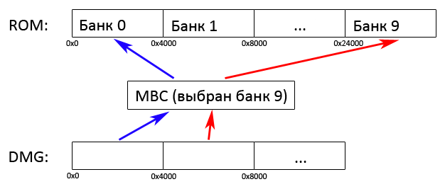
Turning to the addresses 0x4000-0x7FFF, without memory banks, we would get to this address in the image of the game. With the help of memory banks, we can set up so that the image is divided into banks, and at the address 0x4000-0x7FFF the selected bank is displayed. Thus, at one moment in this area there is a second bank, at the other - the tenth. As we want, in general. Thus, we come to virtual and physical addresses. 0x4000-0x7FFF are virtual addresses that do not have to match physical addresses. The physical address is the real address at which the memory is accessed.
All this is necessary so that our DMG can work with images of the game, which far exceed not only 0x8000 bytes, but the entire address space. In words, all this may seem too complicated, but during the implementation it will be clear that these are extremely elementary things that are easier and faster to implement than to explain.
All the same applies to RAM. Banks allow you to expand its volume by placing the chips in the cartridge. In addition, it is possible to implement a full-fledged system of saving, using the built-in battery in the cartridge to power the RAM.
The task of translating a virtual address into a physical one lies on the MBC controller, which is located inside the cartridge. All read and write operations in the ROM area go through it. Also, operations associated with external RAM are redirected here.
Naturally we can not change the contents of the ROM. Write operations are used as control commands for MBC. In the CPU Manual, you can read which addresses are responsible for which functions. Thus, having written the number 9 at a certain address, we say that we want to choose a bank 9. After that, we can read its contents, addressing 0x4000-0x7FFF.
The figure below shows the simplest scheme of the MBC. Here, the area 0x0000-0x3FFF is always redirected to the bank 0, as in some real controllers, while the area 0x4000-0x7FFF is redirected to the current bank.
Consider the DMG address space scheme:
More about each section:
Since the emulator architecture assumes that each DMG component will have its own class, the Cookieboy :: Memory class that emulates memory will contain only the following memory areas - ROM banks, internal RAM 1, Echo of internal RAM 1, Switchable RAM bank, internal RAM 2. When accessing all other areas, the access methods of the corresponding classes will be called.
Let's start with read and write operations in memory. Everything is extremely simple - we look at the address and redirect operations to the corresponding areas of memory. I did as follows. As you can see, many memory areas are well aligned, which allows you to implement everything with the help of switch and logic operations. Here's what it looks like:
And no bulky conventional structures. So far, you can leave only the workpiece, since some memory areas will be in other classes (for example, video memory) that we have not yet implemented. You can only implement what is really in Cookieboy :: Memory. Here you should pay attention to the banks ROM and Switchable RAM bank.
If the cartridge from which the ROM was removed contained an MBC controller, then in these memory areas we need to implement the logic of these controllers. To do this, you can do it very simply - access to these areas is redirected to classes that implement the corresponding MBC controllers, and they themselves let them decide where, how, and what. Consider two examples - MBC 2 and MMM01. The first is as an example that will allow you to realize the rest. MMM01 is a rather odd MBC. There is practically no documentation on it, and its implementation is quite different from other MBCs.It does not hurt to fill this gap in the DMG emulation.
For starters, let's get the base class MBC. It will look like this:
As you can see, the write and read functions come first - they will be called from our Cookieboy :: Memory. Next come the save and load RAM functions. Here we immediately prepare the ground for future emulation of the memory in the cartridge, which is powered from the battery to save its contents after turning off the console. I’ll omit their implementation - it’s just saving and reading the RAMBanks array from the file, no more. Then an extremely obvious constructor and several fields:
The base class is done, now we are going to implement the class that emulates MBC2. Immediately look at the code, and then figure out how this controller works:
Reading is easy. ROMOffset is used as an offset to access the current ROM bank. With RAM there is one detail. MBC2 has 512 4-bit blocks of RAM. We, naturally, select all 512 bytes, just write and read operations truncate values up to 4 low bits.
Now the recording function. This is where the MBC logic is emulated. MBC2 only supports ROM bank change. They change by writing a bank number with a length of 4 bits to the address area 0x2000-0x3FFF. Zero bank can not be selected, because he is already in 0x0000-0x3FFF. It is also worth checking out the ROM. Some games try to choose a bank that does not exist for an indefinite reason. This naturally leads to an error. With the test, the game works as if nothing had happened. One of these games is WordZap. Maybe these are the consequences of inaccurate emulation (I, of course, do not pretend to a perfect DMG emulation), but in any case, verification will not hurt.
Yes, 0xFF is not returned by chance - on the DMG, this value is returned when the content is not defined.
Finally, consider MMM01. I'm not sure about the correctness of my code, since the description of this controller was found on the forum, and it was written by someone unknown. Code:
As you can see, a lot of code. I will not explain each line - after the previous example, I hope that it will not be difficult for you to understand what is being done and why. Let me just say that MMM01 seems to be used in just 2 games, so it’s not by chance that it is not in all emulators.
Returning to the memory emulation, it is worth a little to clarify the memory area called I / O ports. SinceDMG consists of various components, it would be nice to be able to somehow influence their work and even control. To do this, in the memory I / O ports we have access to the registers of all other DMG components: a screen controller, a sound, timers, controls, etc. Naturally, all these registers in our emulator will be in the appropriate classes, which means Cookieboy :: Memory will only redirect all operations in them. A list and purpose of all registers can be found in the CPU Manual. I will also consider them if necessary. By the way, we have already considered one of them - IF. This register is available in this particular area of memory, so you need to redirect read and write operations to the Cookieboy :: Interrupts class. We can already do it, because concerned about this in advance when considering interruptions.
The time has come for another important function - loading a ROM from a file. Before implementing the image loading into memory, it's time to mention what happens when you turn on DMG.
First comes the Bootstrap ROM, which is stored inside the DMG. Its contents can be found in the source code of the Cookieboy :: Memory class. It does nothing special but check the contents of the cartridge and display the Nintendo logo. It has a length of 256 bytes, the execution starts from 0 - i.e. after switching on, the PC processor register is zero. Its execution ends with a command that is written at 0xFF50. At this address is a hidden register that indicates where the commands for the processor are currently coming from — from Bootstrap ROM or the cartridge. Oddly enough, there is almost no description of this register anywhere. Moreover, there is not even a mention of it.
Interesting fact. Bootstrap ROM was received not so long ago, but it was extracted using a photo of a processor chip. The author photographed the part of the processor in which this ROM was located, and by eye one bit counted all the contents.
I note that when you turn on the DMG and cartridge memory contains random numbers. This is an insignificant detail, so emulators usually fill these areas with zeros. What to do - you decide. Most likely, the best or the worst of this game will not work. Remember, it is only about RAM. Filling in with random values of other areas will lead to incorrect operation of the emulator.
Of course, I would not want to run this image every time. To do this, you can do the following. The PC register must be equal to 0x100 - it is at this address that the first team is located in the images of the games. Further, all the processor registers and the I / O ports memory area need to be initialized with the values that Bootstrap ROM leaves behind - these values can be found in the CPU Manual. Not all games are so well written to set all the necessary values on their own, some may rely on the values that are set after performing Bootstrap ROM. To do this, all components contain the EmulateBIOS function, through which all necessary values are set.
And so, we proceed to loading obaraz. The entire image file is read into an array, and the image metadata is read from the header of the image. The most important thing is to know the type of cartridge (type of MBC controller) and the size of external RAM inside the cartridge. Addresses are listed in the CPU Manual. It is also worth implementing the checks that Bootstrap ROM does. Using them, you can easily find out if a file is really a DMG image. The first check is the Nintendo logo. Each ROM contains the Nintendo logo, which is displayed when performing Bootstrap ROM. It must have a strictly defined value. Which one is indicated in the CPU Manual. You can also check the checksum of the image header. To do this, you can use the following code:
If the checks have passed, then we allocate space for the cartridge's RAM and create an object of the corresponding MBC chip.
Regarding the memory of the cartridge, it is a good idea to always have at least one memory bank at hand, even if the image “says” that it is not used. Some games pose as cartridges without MBC, but, nevertheless, they can have a simple chip only for RAM.
Everything is finished with memory.
Not so long ago, an article on the creation of a chip-8 emulator appeared on Habré, thanks to which it was possible to at least superficially understand how emulators are written. After the implementation of your emulator, there was a desire to go further. The choice fell on the original Gameboy. As it turned out, the choice was ideal for a situation when you want to implement something more serious, and the experience of developing emulators is almost absent.
From the point of view of emulation, the Gameboy is relatively simple, but even it requires studying a sufficiently large amount of information. For this reason, several articles will be devoted to the development of the Gameboy emulator. The end result will be an emulator with good compatibility, support for almost all functions of the original, including sound, which is often absent in other emulators. As a bonus, our emulator will run almost all test ROMs, but more on that later.
')
These articles will not contain an exhaustive description of the implementation of the emulator. This is too voluminous, and all the interest from the implementation disappears. Until a specific code will reach only in rare cases. I set myself the task of giving a more theoretical description with a few hints of implementation, which, ideally, should allow you to write your emulator without any particular difficulties and at the same time feel that you wrote it yourself. Where necessary, I will refer to my own implementation - if necessary, you can find the necessary code without having to wade through tons of lines of code.
In this article, we will introduce the Gameboy and begin by emulating its processor and memory.
We write the Gameboy emulator, part 1
We write the Gameboy emulator, part 2
We write the Gameboy emulator, part 3
Table of contents
IntroductionArchitecture
CPU
Interruptions
Memory
Conclusion
Introduction
Gameboy is Nintendo's handheld console, the release of which began in 1989. It will be about the original black and white Gameboy. It is worth noting that in various documents that will guide us, the codename Gameboy is used - DMG (Dot Matrix Game). Further I will use it.
Before you begin, you need to familiarize yourself with the technical characteristics of the DMG:
| CPU | 8-bit Sharp LR35902 operating at 4.19 MHz |
| RAM | 8 KB |
| Video memory | 8 KB |
| Screen resolution | 160x144 |
| Vertical frequency | 59.73 Hz |
| Sound | 4 channels, stereo sound |
After reviewing the test subject, the next step is documentation. The amount of necessary information does not allow to place absolutely everything in the article, so it is necessary to arm yourself with documentation in advance.
For DMG, there is a wonderful document called Gameboy CPU Manual . It includes several well-known documents from eminent developers and contains almost all the information we need. Naturally, this is not all, but at this stage it is more than enough.
Immediately I warn you that there will be mistakes in the documents, even in official ones. During this series of articles, I will try to mention all the shortcomings of various documents that I could find (recall). I will also try to fill many gaps. The bottom line is that there is no exhaustive description for DMG. Available materials give only a superficial idea of the work of many console nodes. If the programmer is not aware of such "pitfalls", then the development of an emulator will become much more difficult than it could be. DMG is quite simple when you have accurate and detailed information on hand. And the problem is that many important details can be learned only from the source code of other emulators, which, nevertheless, does not make our task easier. The code of known emulators is either unnecessarily complicated (Gambatte), or it represents an eerie jumble of, khm, low-quality code (Visual Boy Advance - it’s impossible to look at its code without tears).
Since the articles are written with an eye to my emulator, here is a link to the source code and CookieBoy binary .
Architecture
Let's start with the future architecture of the emulator. To emulate DMG, we will have to implement many modules that are practically independent of each other. In such conditions it would be foolish to go ahead, putting everything in one pile (which is often observed in other emulators. Hi VBA). A more elegant solution is to implement the individual parts of the DMG as separate classes that emulate their parts of iron.I say this for a reason - it was with a jumble of all the components in one superclass that I started developing an emulator. It soon became apparent that things would go much easier further if everyone would only do what they should. Although it should be recognized that in this approach there is an obvious difficulty. You need to have a fairly good understanding of the internal structure of the DMG in order to properly distinguish between the responsibility of classes.
So let's get started.
CPU
DMG contains an 8-bit Sharp LR35902 processor operating at a frequency of 4194304 Hz (no need to be surprised with such accuracy - we will need this number in the future). It can be considered a simplified version of the Zilog Z80 processor, which, in turn, is based on the Intel 8080. Compared with the Z80, some registers and instruction sets are missing.The processor contains eight 8-bit registers A, B, C, D, E, F, H, L and two 16-bit special-purpose registers - PC and SP. Some instructions allow you to combine 8-bit registers and use them as 16-bit registers, namely AF, BC, DE, HL. For example, the BC register is the “glued” registers B and C, where the C register plays the role of the low byte and the B - the high byte.
Registers A, B, C, D, E, H, L are general purpose registers. Register A is also a battery. Register F contains processor flags and is not directly accessible. Below is a diagram of the register. Bits 0 through 3 are not used.
| Bit | 7 | 6 | five | four | 3 | 2 | one | 0 |
| Flag | Z | N | H | C | 0 | 0 | 0 | 0 |
Purpose of flags:
- Zero Flag (Z) - the flag is set (bit is 1) if the result of the last mathematical operation is zero or two operands are equal in comparison.
- Substract Flag (N) - the flag is set if the last operation was subtraction.
- Half Carry Flag (H) - the flag is set if a transfer from the lower half-byte occurred as a result of the last mathematical operation.
- Carry Flag () - the flag is set if a transfer occurred as a result of the last mathematical operation.
The PC register (program counter), as it is easy to guess, is an instruction counter and contains the address of the next instruction.
Register SP (stack pointer), respectively, is a pointer to the top of the stack. For those who do not know, the stack is a memory area in which the values of variables are written, return addresses, and so on. SP contains the address of the top of the stack - the stack grows down, from senior addresses to younger ones. For him, there are always at least two operations. PUSH allows you to insert some value - first, the SP register is reduced, and then the new value is inserted. POP allows you to retrieve a value — first, at the SP address, the value is retrieved from memory, and then the SP is incremented.
The processor also contains the so-called IME (interrupt master enable) - a flag that allows interrupt handling. Accepts, respectively, two values - to prohibit (0) and to permit (1).
With the theory of everything, you can begin to implement. Since we will have to work with both 8-bit registers and their 16-bit pairs, it is advisable to implement a mechanism that allows you to have simultaneous access to those and to those without the need to use bit operations. To do this, declare the following type:
union WordRegister { struct { BYTE L; BYTE H; } bytes; WORD word; }; Processor registers will be stored as pairs, and we will have access to individual parts due to the integration of WordRegister. The “word” field will give access to the entire 16-bit register. The “bytes” field gives access to individual registers in a pair. The only registers A and F should be stored separately. Register A is a battery, which means it is used very often. A similar situation with the register F - processor flags have to be set quite often.
Now let's proceed to the implementation of the processor itself - the Cookieboy :: CPU class will be responsible for this. Reading and executing instructions will be implemented in the usual way - reading an opcode from memory, and then decoding and execution using the switch construction:
BYTE opcode = MMC.Read(PC); PC++; switch (opcode) { case 0x00: break; } All opcodes have a length of 1 byte, but some instructions use a so-called prefix - the first byte is the instruction set prefix (for us, the only prefix is 0xCB), the second byte is the opcode itself from this set. The implementation is elementary - as soon as we stumbled upon 0xCB, we read one more byte and decode it with a nested switch.
This code is placed in the function void Step (), which in one call executes one processor instruction and performs other necessary operations.
Naturally, to read and write to memory, we need another class, Cookieboy :: Memory, whose object can be seen above under the name "MMC". At this stage, a stub with the main methods is enough:
class Memory { public: void Write(WORD addr, BYTE value); BYTE Read(WORD addr); }; The DMG processor has a fairly large number of instructions, a list of which can be found in the Gameboy CPU Manual. It also indicates which processor flags should be set and how many clock cycles the execution of each instruction takes. Very carefully read the description of the flags - incorrectly implemented installation of flags often leads to the inoperability of games, and debugging turns into torture. But I hasten to reassure a little - there are test ROMs for processor flags, but we are still far from the performance of ROMs.
Speaking of clocks. If chip-8 was simple enough, and its emulation did not require taking into account the duration of execution of instructions, then with DMG, the situation is different. Console components do not work as they do, but are synchronized using a clock generator. For us, this means that we need to synchronize the work of all components of our emulator with the processor.
To solve this problem is quite simple. The processor is central to our emulator. Having executed the instruction, we transfer to the other components the time spent by the processor in cycles to synchronize all the components with each other. For this, I use the SYNC_WITH_CPU (clockDelta) macro, to which the processor time spent executing the instruction is passed. It already calls the synchronization functions of the rest of the emulator components. The solution to the synchronization problem could be easily brought out of the processor class, if it were not for one thing.
The components of the console work at the same time, no one waits until the processor finishes executing the instructions, as we do. Some instructions require a long time to execute and in the process data is read and written to memory. The processor, as you can guess, spends a certain time reading / writing memory (4 clock cycles). This leads to the fact that during the execution of the contents of the memory may change, which, of course, it would be nice to emulate too.
In this case, it is necessary to use the synchronization macro several times during the execution so that the correct data is in memory at the moment of its reading or writing. Most instructions do not require such accurate synchronization, and allow it to be performed after execution. Others require an exact sequence of synchronization functions and read / write operations in memory.
It is more correct and more beautiful to do everything differently. We know for sure that each write or read operation from a single byte memory takes 4 clock cycles. It is enough to add auxiliary functions of reading and writing, which themselves call synchronization functions. As soon as this is done, most instructions will immediately acquire the correct duration, because in reality their execution time is made up of just read and write operations. Getting the command opcode also applies here. This is exactly what I did in my emulator, which almost completely freed me from manual synchronization and clock counting. Only a few instructions required my intervention.
And now let's digress a little to clarify the situation with the bars. There is confusion in various documentation. Some documents write such numbers that, for example, the NOP has a duration of 4 cycles, others - 1 cycle (for example, written in the official documentation of Nintendo). To understand the reason it is worth a little distraction from the theory.
Any processor instruction has a certain duration, which we call the machine cycle. In one machine cycle, the processor can perform one action from and to, such as reading an opcode, decoding it and executing a command; read or write value in memory. In turn, the machine cycle consists of machine cycles, since the processor can perform several operations in one machine cycle. And here we come to our processor. If we say that the NOP lasts 4 bars, then we are talking about machine cycles. If we are talking about 1 tick for NOP, then we are talking about machine cycles. The DMG processor works exactly like this - its machine cycle lasts 4 machine cycles and many instructions have a duration of exactly 4 cycles or 1 machine cycle - the DMG processor is able to read the opcode from memory, decode it and execute the instruction in just 4 machine cycles.
Hereinafter I will use more familiar machine cycles. They correspond to one period of the clock generator, which means that they are the minimum and indivisible unit of time for our emulator. Thus, the NOP operation will last 4 clocks.
At this stage it is already possible to fully implement the emulation of all processor commands. We should also mention some of them:
- HALT has quite an interesting behavior, which is described in the CPU Manual (2.7.3. Low-Power Mode). A solution to the forehead will result in the test of the HALT instruction not being passed. Here you need to be careful both in the implementation of the instruction itself and in the implementation of the interrupt handler (more on this later). The implementation of the instruction is such that it does not suspend execution and leads to the mentioned bug only if the IME is zero and there are currently no interrupts that need to be processed (more on this later) - the last moment is omitted in most documents. Otherwise, there is no bug, and the execution is suspended. Naturally, the clock generator and all other components continue their work, which means that it is necessary to continue to call synchronization functions, giving 4 clock cycles as an argument (it makes no sense to count in this mode by one clock cycle). As if the processor executes the NOP.
- In POP AF it is worth considering the fact that there are unused bits in the F register. To do this, you need to clear the lower 4 bits of register F after its contents have been removed from the stack.
- The RLCA, RLA, RRCA, RRA instructions always reset the Z flag in the F register.
In addition to these shortcomings, there are others. The CPU Manual contains an incomplete description of the duration of the instructions. As you might guess, conditional branch instructions should have different lengths depending on whether the transition occurred or not. It would be possible to use test ROMs, but they do not work by themselves because of these instructions, so they generate an unknown error without even starting testing. Here is a table of these instructions, indicating their duration:
| Opcodes | Transition did not occur | Transition has occurred |
| 0xC2, 0xCA, 0xD2, 0xDA | 12 | sixteen |
| 0x20, 0x28, 0x30, 0x38 | eight | 12 |
| 0xC4, 0xCC, 0xD4, 0xDC | 12 | 24 |
| 0xC0, 0xC8, 0xD0, 0xD8 | eight | 20 |
Also for the RST n instructions (opcodes 0xC7, 0xCF, 0xD7, 0xDF, 0xE7, 0xEF, 0xF7, 0xFF) the wrong duration is specified. The correct value is 16 bars.
And so, at the moment our “processor” is able to read instructions from memory, execute them and synchronize other components with itself (as it were, it synchronizes until all these functions are dummies). After that, we need to check whether there was an interruption after all the work done.
Interruptions
An interrupt is an event that pauses the execution of the current instructions of the processor and transfers control to the interrupt handler. DMG works on this principle.During synchronization, we call synchronization methods of other components of the emulator that can request an interrupt. In DMG, this is done as follows. There are two registers (where they will be discussed below) - IF (interrupt flags) and IE (interrupt enable). Their bits have a specific purpose, which is identical in both registers:
| Bit | Interrupt |
| four | Joypad |
| 3 | Serial I / O transfer complete |
| 2 | Timer overflow |
| one | LCDC |
| 0 | V-blank |
The IF register bits indicate which interrupts were requested. If the bit is set, the interrupt is requested.
IE register bits enable interrupt handling. If the bit is set to one and the corresponding interrupt has been requested, it will be processed. If not, the interrupt will not be processed.
As you can see, the identical assignment of bits is very handy and allows using the logical operation AND to find out which interrupts should be processed.
One important detail is that the interrupt brings the processor out of a stall state, resulting from the execution of a HALT or STOP. And here the algorithm by which the interrupt registers are checked is very important. The algorithm is as follows:
- We check if there are any interrupts that should be processed. This is done using the logical AND operation between the IE and IF registers. It is also worthwhile to perform a logical AND operation with the result and the number 0x1F to remove possible garbage, since the upper three bits are not used in both registers.
- If there are no such interruptions, then exit the function. If they are, then right now we have to bring the processor out of the stop state.
- Now we start interrupt handling. To do this, we check if the IME flag prohibits their processing. If not, then:
- reset IME;
- load the PC register onto the stack;
- call the interrupt handler by setting the PC register to the address of the handler in memory;
- reset the IF register bit according to the processed interrupt.
Interrupts are processed one at a time and in a strictly defined order. All information about the priorities and addresses of handlers is listed in the CPU Manual.
An important detail. Again, a thought might already have occurred to someone — an interrupt handling is very similar to a procedure call, which means it should take some time. This is indeed the case and it takes 20 clock cycles. For some reason, this moment is omitted in documents describing DMG.
Now we proceed to the implementation. Interrupts will be handled by the class Cookieboy :: Interrupts. In it, we put the IE and IF registers and declare functions for accessing these registers (we will need them later), as well as a function that allows you to request a specific interrupt (we don’t want to manipulate bits every time to request an interrupt) . We also need a function that will check which interrupts are worth processing. We place a call to this function at the end of the processor's Step function and additionally synchronize the components.
A little about the interrupt request. It is done by setting the corresponding bits in the IF register. Before installing, checking the register of IE is not required. Even if the bits in it prohibit a specific interrupt, we still set the bits in the IF register for that interrupt.
If you looked at the source code of my implementation of Cookieboy :: Interrupts, you might notice that I return the value of the IE and IF registers after I set to 1 all unused bits in them (OR operation with the value 0xE0). I do it for a reason. Many registers in the I / O ports (about this below) use not all bits, others restrict read access to some bits or the entire register at once. It is also necessary to take into account - for this, the unused and prohibited for reading bits should be set to 1 before returning.
Let's sum up. Our emulator is able to execute instructions of the processor, synchronizes all components of the emulator with each other, handles interrupts. True, it's all just in words. To get a really working emulator, we need to emulate DMG memory.
Memory
We define one term in advance - the memory bank. By this is meant the memory area of a strictly defined size. There are two types of banks - ROM banks having a length of 0x4000 bytes, and RAM banks having a length of 0x2000 (once you get used to the hexadecimal number system, it will be easier for me and you). Why do you need it? The DMG processor is capable of working with 16-bit addresses, which means that the address space is limited to 0x10000 bytes. Of these, only 0x8000 bytes is allocated to the image of the game. In most cases, this is not enough and memory banks take over.Turning to the addresses 0x4000-0x7FFF, without memory banks, we would get to this address in the image of the game. With the help of memory banks, we can set up so that the image is divided into banks, and at the address 0x4000-0x7FFF the selected bank is displayed. Thus, at one moment in this area there is a second bank, at the other - the tenth. As we want, in general. Thus, we come to virtual and physical addresses. 0x4000-0x7FFF are virtual addresses that do not have to match physical addresses. The physical address is the real address at which the memory is accessed.
All this is necessary so that our DMG can work with images of the game, which far exceed not only 0x8000 bytes, but the entire address space. In words, all this may seem too complicated, but during the implementation it will be clear that these are extremely elementary things that are easier and faster to implement than to explain.
All the same applies to RAM. Banks allow you to expand its volume by placing the chips in the cartridge. In addition, it is possible to implement a full-fledged system of saving, using the built-in battery in the cartridge to power the RAM.
The task of translating a virtual address into a physical one lies on the MBC controller, which is located inside the cartridge. All read and write operations in the ROM area go through it. Also, operations associated with external RAM are redirected here.
Naturally we can not change the contents of the ROM. Write operations are used as control commands for MBC. In the CPU Manual, you can read which addresses are responsible for which functions. Thus, having written the number 9 at a certain address, we say that we want to choose a bank 9. After that, we can read its contents, addressing 0x4000-0x7FFF.
The figure below shows the simplest scheme of the MBC. Here, the area 0x0000-0x3FFF is always redirected to the bank 0, as in some real controllers, while the area 0x4000-0x7FFF is redirected to the current bank.
Consider the DMG address space scheme:
| Memory section | Starting address | End address |
| ROM bank 0 | 0x0000 | 0x3FFF |
| Switchable ROM bank | 0x4000 | 0x7FFF |
| Video RAM | 0x8000 | 0x9FFF |
| Switchable RAM bank | 0xA000 | 0xBFFF |
| Internal RAM 1 | 0xC000 | 0xDFFF |
| Echo of Internal RAM 1 | 0xE000 | 0xFDFF |
| Oam | 0xFE00 | 0xFE9F |
| Not used | 0xFEA0 | 0xFEFF |
| I / O ports | 0xFF00 | 0xFF4B |
| Not used | 0xFF4C | 0xFF7F |
| Internal RAM 2 | 0xFF80 | 0xFFFE |
| Interrupt enable register | 0xFFFF | 0xFFFF |
More about each section:
- ROM bank 0. Switchable ROM bank. We have already reviewed these areas.
- Video RAM. More will be considered when implementing graphics.
- Internal RAM 1. RAM inside DMG.
- Echo of Internal RAM 1. The contents of Internal RAM 1 are duplicated here.
- Oam Here is a description of the sprites.
- I / O ports. Here we get access to the registers of other DMG components.
- Internal RAM 2. RAM inside DMG.
- Interrupt enable register. This register stores flags that allow the handling of certain interrupts. This is the same IE register that we already talked about.
Since the emulator architecture assumes that each DMG component will have its own class, the Cookieboy :: Memory class that emulates memory will contain only the following memory areas - ROM banks, internal RAM 1, Echo of internal RAM 1, Switchable RAM bank, internal RAM 2. When accessing all other areas, the access methods of the corresponding classes will be called.
Let's start with read and write operations in memory. Everything is extremely simple - we look at the address and redirect operations to the corresponding areas of memory. I did as follows. As you can see, many memory areas are well aligned, which allows you to implement everything with the help of switch and logic operations. Here's what it looks like:
switch (addr & 0xF000) { case 0x8000: case 0x9000: // break; } And no bulky conventional structures. So far, you can leave only the workpiece, since some memory areas will be in other classes (for example, video memory) that we have not yet implemented. You can only implement what is really in Cookieboy :: Memory. Here you should pay attention to the banks ROM and Switchable RAM bank.
If the cartridge from which the ROM was removed contained an MBC controller, then in these memory areas we need to implement the logic of these controllers. To do this, you can do it very simply - access to these areas is redirected to classes that implement the corresponding MBC controllers, and they themselves let them decide where, how, and what. Consider two examples - MBC 2 and MMM01. The first is as an example that will allow you to realize the rest. MMM01 is a rather odd MBC. There is practically no documentation on it, and its implementation is quite different from other MBCs.It does not hurt to fill this gap in the DMG emulation.
For starters, let's get the base class MBC. It will look like this:
const int ROMBankSize = 0x4000; const int RAMBankSize = 0x2000; class MBC { public: virtual void Write(WORD addr, BYTE value) = 0; virtual BYTE Read(WORD addr) = 0; virtual bool SaveRAM(const char *path, DWORD RAMSize); virtual bool LoadRAM(const char *path, DWORD RAMSize); protected: MBC(BYTE *ROM, DWORD ROMSize, BYTE *RAMBanks, DWORD RAMSize) : ROM(ROM), ROMSize(ROMSize), RAMBanks(RAMBanks), RAMSize(RAMSize) {} BYTE *ROM; BYTE *RAMBanks; DWORD ROMOffset; DWORD RAMOffset; DWORD ROMSize; DWORD RAMSize; }; As you can see, the write and read functions come first - they will be called from our Cookieboy :: Memory. Next come the save and load RAM functions. Here we immediately prepare the ground for future emulation of the memory in the cartridge, which is powered from the battery to save its contents after turning off the console. I’ll omit their implementation - it’s just saving and reading the RAMBanks array from the file, no more. Then an extremely obvious constructor and several fields:
- ROM. Here we have the whole image of the game.
- RAMBanks. Here is the memory of the cartridge.
- RAMOffset and ROMOffset. These are offsets that indicate the current memory bank.
- ROMSize and RAMSize, I think, do not require explanation. Values are stored in memory banks, not in bytes.
The base class is done, now we are going to implement the class that emulates MBC2. Immediately look at the code, and then figure out how this controller works:
class MBC2 : public MBC { public: MBC2(BYTE *ROM, DWORD ROMSize, BYTE *RAMBanks, DWORD RAMSize) : MBC(ROM, ROMSize, RAMBanks, RAMSize) { ROMOffset = ROMBankSize; RAMOffset = 0; } virtual void Write(WORD addr, BYTE value) { switch (addr & 0xF000) { //ROM bank switching case 0x2000: case 0x3000: ROMOffset = value & 0xF; ROMOffset %= ROMSize; if (ROMOffset == 0) { ROMOffset = 1; } ROMOffset *= ROMBankSize; break; //RAM bank 0 case 0xA000: case 0xB000: RAMBanks[addr - 0xA000] = value & 0xF; break; } } virtual BYTE Read(WORD addr) { switch (addr & 0xF000) { //ROM bank 0 case 0x0000: case 0x1000: case 0x2000: case 0x3000: return ROM[addr]; //ROM bank 1 case 0x4000: case 0x5000: case 0x6000: case 0x7000: return ROM[ROMOffset + (addr - 0x4000)]; //RAM bank 0 case 0xA000: case 0xB000: return RAMBanks[addr - 0xA000] & 0xF; } return 0xFF; } }; Reading is easy. ROMOffset is used as an offset to access the current ROM bank. With RAM there is one detail. MBC2 has 512 4-bit blocks of RAM. We, naturally, select all 512 bytes, just write and read operations truncate values up to 4 low bits.
Now the recording function. This is where the MBC logic is emulated. MBC2 only supports ROM bank change. They change by writing a bank number with a length of 4 bits to the address area 0x2000-0x3FFF. Zero bank can not be selected, because he is already in 0x0000-0x3FFF. It is also worth checking out the ROM. Some games try to choose a bank that does not exist for an indefinite reason. This naturally leads to an error. With the test, the game works as if nothing had happened. One of these games is WordZap. Maybe these are the consequences of inaccurate emulation (I, of course, do not pretend to a perfect DMG emulation), but in any case, verification will not hurt.
Yes, 0xFF is not returned by chance - on the DMG, this value is returned when the content is not defined.
Finally, consider MMM01. I'm not sure about the correctness of my code, since the description of this controller was found on the forum, and it was written by someone unknown. Code:
class MBC_MMM01 : public MBC { public: enum MMM01ModesEnum { MMM01MODE_ROMONLY = 0, MMM01MODE_BANKING = 1 }; MBC_MMM01(BYTE *ROM, DWORD ROMSize, BYTE *RAMBanks, DWORD RAMSize) : MBC(ROM, ROMSize, RAMBanks, RAMSize) { ROMOffset = ROMBankSize; RAMOffset = 0; RAMEnabled = false; Mode = MMM01MODE_ROMONLY; ROMBase = 0x0; } virtual void Write(WORD addr, BYTE value) { switch (addr & 0xF000) { //Modes switching case 0x0000: case 0x1000: if (Mode == MMM01MODE_ROMONLY) { Mode = MMM01MODE_BANKING; } else { RAMEnabled = (value & 0x0F) == 0x0A; } break; //ROM bank switching case 0x2000: case 0x3000: if (Mode == MMM01MODE_ROMONLY) { ROMBase = value & 0x3F; ROMBase %= ROMSize - 2; ROMBase *= ROMBankSize; } else { if (value + ROMBase / ROMBankSize > ROMSize - 3) { value = (ROMSize - 3 - ROMBase / ROMBankSize) & 0xFF; } ROMOffset = value * ROMBankSize; } break; //RAM bank switching in banking mode case 0x4000: case 0x5000: if (Mode == MMM01MODE_BANKING) { value %= RAMSize; RAMOffset = value * RAMBankSize; } break; //Switchable RAM bank case 0xA000: case 0xB000: if (RAMEnabled) { RAMBanks[RAMOffset + (addr - 0xA000)] = value; } break; } } virtual BYTE Read(WORD addr) { if (Mode == MMM01MODE_ROMONLY) { switch (addr & 0xF000) { //ROM bank 0 case 0x0000: case 0x1000: case 0x2000: case 0x3000: //ROM bank 1 case 0x4000: case 0x5000: case 0x6000: case 0x7000: return ROM[addr]; //Switchable RAM bank case 0xA000: case 0xB000: if (RAMEnabled) { return RAMBanks[RAMOffset + (addr - 0xA000)]; } } } else { switch (addr & 0xF000) { //ROM bank 0 case 0x0000: case 0x1000: case 0x2000: case 0x3000: return ROM[ROMBankSize * 2 + ROMBase + addr]; //ROM bank 1 case 0x4000: case 0x5000: case 0x6000: case 0x7000: return ROM[ROMBankSize * 2 + ROMBase + ROMOffset + (addr - 0x4000)]; //Switchable RAM bank case 0xA000: case 0xB000: if (RAMEnabled) { return RAMBanks[RAMOffset + (addr - 0xA000)]; } } } return 0xFF; } private: bool RAMEnabled; MMM01ModesEnum Mode; DWORD ROMBase; }; As you can see, a lot of code. I will not explain each line - after the previous example, I hope that it will not be difficult for you to understand what is being done and why. Let me just say that MMM01 seems to be used in just 2 games, so it’s not by chance that it is not in all emulators.
Returning to the memory emulation, it is worth a little to clarify the memory area called I / O ports. SinceDMG consists of various components, it would be nice to be able to somehow influence their work and even control. To do this, in the memory I / O ports we have access to the registers of all other DMG components: a screen controller, a sound, timers, controls, etc. Naturally, all these registers in our emulator will be in the appropriate classes, which means Cookieboy :: Memory will only redirect all operations in them. A list and purpose of all registers can be found in the CPU Manual. I will also consider them if necessary. By the way, we have already considered one of them - IF. This register is available in this particular area of memory, so you need to redirect read and write operations to the Cookieboy :: Interrupts class. We can already do it, because concerned about this in advance when considering interruptions.
The time has come for another important function - loading a ROM from a file. Before implementing the image loading into memory, it's time to mention what happens when you turn on DMG.
First comes the Bootstrap ROM, which is stored inside the DMG. Its contents can be found in the source code of the Cookieboy :: Memory class. It does nothing special but check the contents of the cartridge and display the Nintendo logo. It has a length of 256 bytes, the execution starts from 0 - i.e. after switching on, the PC processor register is zero. Its execution ends with a command that is written at 0xFF50. At this address is a hidden register that indicates where the commands for the processor are currently coming from — from Bootstrap ROM or the cartridge. Oddly enough, there is almost no description of this register anywhere. Moreover, there is not even a mention of it.
Interesting fact. Bootstrap ROM was received not so long ago, but it was extracted using a photo of a processor chip. The author photographed the part of the processor in which this ROM was located, and by eye one bit counted all the contents.
I note that when you turn on the DMG and cartridge memory contains random numbers. This is an insignificant detail, so emulators usually fill these areas with zeros. What to do - you decide. Most likely, the best or the worst of this game will not work. Remember, it is only about RAM. Filling in with random values of other areas will lead to incorrect operation of the emulator.
Of course, I would not want to run this image every time. To do this, you can do the following. The PC register must be equal to 0x100 - it is at this address that the first team is located in the images of the games. Further, all the processor registers and the I / O ports memory area need to be initialized with the values that Bootstrap ROM leaves behind - these values can be found in the CPU Manual. Not all games are so well written to set all the necessary values on their own, some may rely on the values that are set after performing Bootstrap ROM. To do this, all components contain the EmulateBIOS function, through which all necessary values are set.
And so, we proceed to loading obaraz. The entire image file is read into an array, and the image metadata is read from the header of the image. The most important thing is to know the type of cartridge (type of MBC controller) and the size of external RAM inside the cartridge. Addresses are listed in the CPU Manual. It is also worth implementing the checks that Bootstrap ROM does. Using them, you can easily find out if a file is really a DMG image. The first check is the Nintendo logo. Each ROM contains the Nintendo logo, which is displayed when performing Bootstrap ROM. It must have a strictly defined value. Which one is indicated in the CPU Manual. You can also check the checksum of the image header. To do this, you can use the following code:
BYTE Complement = 0; for (int i = 0x134; i <= 0x14C; i++) { Complement = Complement - ROM[i] - 1; } if (Complement != ROM[0x14D]) { // } If the checks have passed, then we allocate space for the cartridge's RAM and create an object of the corresponding MBC chip.
Regarding the memory of the cartridge, it is a good idea to always have at least one memory bank at hand, even if the image “says” that it is not used. Some games pose as cartridges without MBC, but, nevertheless, they can have a simple chip only for RAM.
Everything is finished with memory.
Conclusion
For the introductory article, we have done a lot of work, but this is not even half of what we need. At the moment, our emulator is able to read the image and execute its code. Most importantly, he can really do all this. Naturally, we see nothing on the screen. This is what we will fix in the next article.Source: https://habr.com/ru/post/154901/
All Articles