FPGA is simple or do it yourself
On Habré, there are many articles devoted to microcontrollers and programming languages on them, but not often you can find articles on programming FPGAs. FPGA firmware can be written in hardware description languages or you can draw diagrams in CAD programs of FPGA companies. Today I want to show how to program the ALU on an FPGA by Actel A3P250 (ProASIC 3 with a number of equivalent gates of 250,000) in the language of hardware description SystemVerilog. This FPGA is interesting because it allows you to prototype custom-made ASIC or BMC chips. The firmware that is synthesized for this FPGA can be turned with a serial chip.
Who cares welcome under cat.
So, the creation of the firmware can be divided into several stages:
1. Determine what we want to get, draw on a piece of paper, in the head or in Visio a block diagram of the future device. In my case it is an ALU, it has inputs: two operands of 4 bits each, a reset input, a synchronization input, an operation code input 2 bits (00 is addition, 01 is subtraction, 10 is multiplication, 11 is the result is 0) and output is the result of 8 discharges.
2. If the project is complex, then it is necessary to write a behavioral model, in some high-level language, for example in C #, by which you can understand how it will work, in this case I’ll skip this point, because I’ll write a model in C or C This device will be able to many, and I'm sure better than me.
3. Actually we write code, I use NPP with SystemVerilog syntax highlighting for this, although you can write in any text editor or in one of the programs for modeling, synthesizing or tracing the chip, but more on that later.
The firmware code at this stage I will call the logical model, although it may be different in different sources.
4. We write a test for our logical model, for this we can use several methods. Also at this stage we combine test and model.
5. Run our model with a test in the modeling environment. I use QuestaSim for modeling, this is an advanced version of ModelSim from Mentor Graphics.
6. If the tests are performed successfully, then you can proceed to the synthesis. For synthesis, I use Mentor Graphics Precision Synthesis. But you can use the software that the chip manufacturer provides you. As a result of the synthesis, we get files in the format * .edf and Verilog, this is a logical model assembled by CAD synthesis from those blocks that are in the FPGA, as well as a description of the connections between them. I will call these files no-lists.
7. The file of the no-list in the Verilog format must be connected instead of the logical model and the simulation must be restarted to make sure that the synthesis was successful and the synthesizer did not throw out anything extra, he knows it very well. Also at this stage, you can use the means of formal verification, which will verify the compliance of the resulting no-list of the logical model.
8. If the no-list has been tested, you can proceed to the placement and tracing of the no-list in the FPGA, for this I will use Actel Designer, which is part of the Actel Libero IDE. At this stage, we get the finished firmware FPGA and, just as important, the revised no-list and time delays in its circuits, the no-list again has the Verilog format, and the delays are generated in the * .sdf format.
9. Now you need to simulate the no-list obtained as a result of tracing with time delays and make sure that everything works.
10. If everything really works, then you can flash it.
')
Now back to the ALU.
The code in SystemVerilog consists of modules, at least in that part, as regards the description of the equipment, since When testing, the keywords class and program appear.
As it is not sad, but the tag for SystemVerilog or at least Verilog is not, but there is a tag for VHDL, I had to use it ...
We analyze the module ALU in parts.
First we announce the name of the module and the inputs / outputs, remember we defined them at the first stage.
Then we declare several internal lines for connecting the combinational part and the trigger part.
Now we will describe combinational or asynchronous often ALU:
And finally, the trigger or synchronous part of the ALU, because the ALU will be synchronous
Module close the keyword:
Now we will write a test and run the simulation, we get the following timing diagram:
As we can see, operations are performed, but because of two triggers at the input and output, we get a delay of 2 clocks, this can be corrected, but we simply consider an example and do not create a Core i7, so let's leave it and proceed to the synthesis:
The synthesizer decided that our circuit would look like the figure above, in general, I agree with him here, although this is not always the case and therefore I will not even run the test once more immediately proceed to the trace in the crystal.
Since I have a whale design, then I will place the conclusions of the FPGA as follows:
The result of the work of the router (placement of elements in the crystal) in the figure below, by the way at this stage, you can move the elements around the crystal.
Yellow highlighted circuit clock signal.
At this point I want to finish my story, the video will be later.
Thanks to everyone who read to the end, I apologize for the style and possible errors in the text, but I'm not a writer just learning.
PS To whom it is interesting PLIS I have been doing for 3 years already, this project of the ALU was made in an hour, it was necessary to have a simple layout for checking one method of introducing failures.
Who cares welcome under cat.
So, the creation of the firmware can be divided into several stages:
1. Determine what we want to get, draw on a piece of paper, in the head or in Visio a block diagram of the future device. In my case it is an ALU, it has inputs: two operands of 4 bits each, a reset input, a synchronization input, an operation code input 2 bits (00 is addition, 01 is subtraction, 10 is multiplication, 11 is the result is 0) and output is the result of 8 discharges.
2. If the project is complex, then it is necessary to write a behavioral model, in some high-level language, for example in C #, by which you can understand how it will work, in this case I’ll skip this point, because I’ll write a model in C or C This device will be able to many, and I'm sure better than me.
3. Actually we write code, I use NPP with SystemVerilog syntax highlighting for this, although you can write in any text editor or in one of the programs for modeling, synthesizing or tracing the chip, but more on that later.
The firmware code at this stage I will call the logical model, although it may be different in different sources.
4. We write a test for our logical model, for this we can use several methods. Also at this stage we combine test and model.
5. Run our model with a test in the modeling environment. I use QuestaSim for modeling, this is an advanced version of ModelSim from Mentor Graphics.
6. If the tests are performed successfully, then you can proceed to the synthesis. For synthesis, I use Mentor Graphics Precision Synthesis. But you can use the software that the chip manufacturer provides you. As a result of the synthesis, we get files in the format * .edf and Verilog, this is a logical model assembled by CAD synthesis from those blocks that are in the FPGA, as well as a description of the connections between them. I will call these files no-lists.
7. The file of the no-list in the Verilog format must be connected instead of the logical model and the simulation must be restarted to make sure that the synthesis was successful and the synthesizer did not throw out anything extra, he knows it very well. Also at this stage, you can use the means of formal verification, which will verify the compliance of the resulting no-list of the logical model.
8. If the no-list has been tested, you can proceed to the placement and tracing of the no-list in the FPGA, for this I will use Actel Designer, which is part of the Actel Libero IDE. At this stage, we get the finished firmware FPGA and, just as important, the revised no-list and time delays in its circuits, the no-list again has the Verilog format, and the delays are generated in the * .sdf format.
9. Now you need to simulate the no-list obtained as a result of tracing with time delays and make sure that everything works.
10. If everything really works, then you can flash it.
')
Now back to the ALU.
The code in SystemVerilog consists of modules, at least in that part, as regards the description of the equipment, since When testing, the keywords class and program appear.
As it is not sad, but the tag for SystemVerilog or at least Verilog is not, but there is a tag for VHDL, I had to use it ...
We analyze the module ALU in parts.
First we announce the name of the module and the inputs / outputs, remember we defined them at the first stage.
module ALU ( input rst, clk, // input [1:0] cmd, // input [3:0] a,b, // output logic [7:0] res // ); Then we declare several internal lines for connecting the combinational part and the trigger part.
logic [3:0] A, B; logic [1:0] Cmd; logic [7:0] outpRes; Now we will describe combinational or asynchronous often ALU:
always_comb begin unique case(Cmd) 2'b00: begin:add outpRes = A+B; end:add 2'b01: begin:sub outpRes = AB; end:sub 2'b10: begin:mul outpRes = A*B; end:mul 2'b11: begin:div outpRes = 0; end:div endcase end And finally, the trigger or synchronous part of the ALU, because the ALU will be synchronous
always_ff @(posedge clk, posedge rst) if (rst) begin res <= '0; A <='0; B <='0; Cmd <='0; end else begin A[3:0] <= a; B[3:0] <= b; Cmd <=cmd; res <= outpRes; end Module close the keyword:
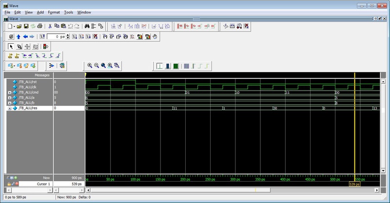
endmodule Now we will write a test and run the simulation, we get the following timing diagram:
As we can see, operations are performed, but because of two triggers at the input and output, we get a delay of 2 clocks, this can be corrected, but we simply consider an example and do not create a Core i7, so let's leave it and proceed to the synthesis:
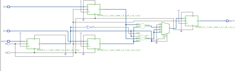
The synthesizer decided that our circuit would look like the figure above, in general, I agree with him here, although this is not always the case and therefore I will not even run the test once more immediately proceed to the trace in the crystal.
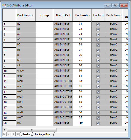
Since I have a whale design, then I will place the conclusions of the FPGA as follows:
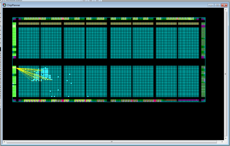
The result of the work of the router (placement of elements in the crystal) in the figure below, by the way at this stage, you can move the elements around the crystal.
Yellow highlighted circuit clock signal.
At this point I want to finish my story, the video will be later.
Thanks to everyone who read to the end, I apologize for the style and possible errors in the text, but I'm not a writer just learning.
PS To whom it is interesting PLIS I have been doing for 3 years already, this project of the ALU was made in an hour, it was necessary to have a simple layout for checking one method of introducing failures.
Source: https://habr.com/ru/post/152491/
All Articles