Manually flash AVR

Picture to attract attention - xkcd
Imagine that you are on a desert island. And you vital need to program the microcontroller. Why, you ask? Well, let's say, to fix an emergency radio beacon, without which the chances of rescue fall sharply.
Rejoicing that you have not yet forgotten the assembly course, you somehow wrote a program with a stick in the sand. Among the surviving things, by some miracle, there was a printout of documentation for the controller (well, that you have not had time to put it on the kindling!), And the program was converted into machine codes. It remains the very nonsense - to flash it into the controller. But within a radius of 500 kilometers there is not a single programmer, not to mention computers. You have only a power source (a battery of coconut
')
How to flash the MK with bare hands?
As the experimental will be MK ATtiny13 company Atmel. The described method works with almost any controller of the AVR family, except that the command codes may differ slightly.
Interface
The most common and convenient interface for AVR firmware is the SPI (Serial Peripheral Interface). To connect via SPI you need only four wires, not including ground:- SCK - clock signal, synchronizes all data exchange operations;
- MOSI (Master Out Slave In) - data line from master to slave;
- MISO (Master In Slave Out) - data line, on the contrary, from the slave to the master;
- RESET - to enable SPI firmware, you must apply a logical "0" to this output.
Thus, we need to form three signals and (optionally) read one. Here is the simplest scheme for this:
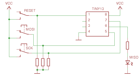
Fig. 1. The simplest SPI connection scheme.
For your own convenience, you can add an indication of the input signals. The scheme is complicated, but not excessive:

Fig. 2. Scheme with indication of signals.
Chatter protection
Unfortunately, simply using the buttons to form SPI signals, we will not achieve a good result. The reason for this is an unpleasant phenomenon called contact bounce . During the closure, the mechanical contacts collide, bounce off each other, and instead of one impulse, several are obtained. To suppress the chatter, you will have to assemble a simple circuit of a pair of logical elements:

Fig. 3. RS trigger for chatter suppression.
This is an RS trigger that switches to state “1” at the moment of closing the lower contact of the switch and ignores other bounce pulses. Resetting the trigger back to “0” occurs when the upper contact is closed, that is, when the button is released.
“Look, run away!” The reader will say, “I’m sitting on a desert island. Where am I going to get the triggers? ”Well, you can get rid of the bounce and without electronic circuits. It is only necessary to replace the “dry” contact with a
MOSI and RESET signals do not require chatter suppression, unlike SCK: here the signal level only has the signal level at the time of the sample, and not its edges.
How does SPI work

Fig. 4. Timing diagram of SPI.
SPI is a synchronous interface: all operations are synchronized with clock edges (SCK), which is generated by the master. The maximum transfer rate is limited to 1/4 of the clock frequency of the controller. There is no limit on the minimum speed: without a clock signal, data exchange is “frozen”, and the interface can remain in a static state for an arbitrarily long time.
Transmission over SPI is done in full duplex mode, one bit per clock per direction. On the rising edge of the SCK signal, the slave device reads the next bit from the MOSI line, and on the falling edge it outputs the next bit to the MISO line. All attention to Figure 4.
Firmware protocol
All communication of the programmer with the MC consists of sending 32-bit commands and receiving controller responses. A full list of commands is in the datasheet, and here we will list what operations need to be performed for the MK firmware:- Putting the controller into programming mode;
- (optional) Read device identifier;
- Erasing;
- Record in flash;
- (optional) Check recorded;
Consider each step in detail.
Enable programming mode
Programming mode is activated by applying “0” to RESET leg. But there are some subtleties. Atmel recommends that you first put a low level on the RESET and SCK outputs, and only then supply power to the controller. If this is not possible, after powering up, apply “0” to SCK, and then a positive impulse to RESET:

Fig. 5. Transfer MK in programming mode.
But that's not all. Next, you need to send a command to actually enable the programming mode: 10101100 01010011 xxxxxxxx xxxxxxxx
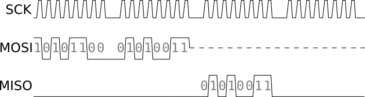
Fig. 6. “Program Enable” command.
Bits labeled x can be any. During the transmission of the third byte, the controller must send back the second byte ( 01010011 ). If this happens, then all is well, the command is accepted, the controller is waiting for further instructions. If the answer is different, you need to restart the MC and try it all over again.
ID verification

Fig. 7. Team "Read Signature Byte".
Before you write anything in the memory of the MK, you need to make sure that we have exactly the model we need. Each controller model has its own three-byte identifier (Signature). You can read it with commands like
00110000 000xxxxx xxxxxxbb xxxxxxxx
Instead of bb (third byte of the command), substitute 00 for the first byte of the identifier, 01 for the second and 10 for the third. The corresponding identifier byte will be transmitted by the controller when sending the 4th byte of the command.
For ATtiny13, the identifier value is 00011110 10010000 00000111 ( 0x1E 90 07 ).
Controller cleaning

Fig. 8. Team "Chip Erase".
The next step is to clear the memory MK, which is carried out by sending the command "Chip Erase"
10101100 100xxxxx xxxxxxxx xxxxxxxx
This command will erase the contents of Flash and EEPROM (all cells will contain FF), as well as removing lock bits, if they are set.
Write to flash memory
The program memory (Flash) in ATtiny13 consists of 512 double-byte words (1K bytes). The word address is 9 bits wide. Flash-memory is divided into pages, each page has a size of 16 words (a total of 32 pages). Recording in flash is carried out in two stages.
First you need to load data into the page buffer, for this you use the command “Load Program Memory Page”
01000000 000xxxxx xxxxbbbb iiiiiiii - to load the low byte of the word, and 01001000 000xxxxx xxxxbbbb iiiiiiii - to load the high byte.
The 4 low bits of the 3rd byte of the bbbb command are the address of the word on the page, iiiiiiii is the download byte. First, the low byte of the word must always be loaded, and then the high byte of the same word.

Fig. 9. “Load Program Memory Page” command.
After the page buffer has been loaded, the “Write Program Memory Page” 01001100 0000000a bbbbxxxx xxxxxxxx command must be executed to write the page directly to the controller's memory.
The low bit of the second byte and the high 4 bits of the third a: bbbb is the five-bit page number to write.

Fig. 10. “Write Program Memory Page” command.
It all looks rather confusing, but nothing complicated. The address of any byte of program memory consists of 10 bits: ppppp: bbbb: w , where
ppppp - page number (used in the “Write Program Memory Page” command);
bbbb - the address of the word on the page (in the command “Load Program Memory Page”);
w - a bit that identifies the high or low byte in the word (encrypted in the first byte of the “Load Program Memory Page” command).
Reading flash

Fig. 11. The “Read Program Memory” command.
After writing the firmware to the MC, it would be nice to check what was written, since no data integrity check was performed. The only way to check is to read the entire amount of flash-memory and compare with the original.
Reading the program memory is easier than writing to it. Forget about page organization, reading is performed byte-by-byte. The “Read Program Memory” command looks like this:
00100000 0000000a bbbbbbbb xxxxxxxx is for reading the low byte of a word, and 00101000 0000000a bbbbbbbb xxxxxxxx is for the high byte.
The low bit of the second byte and the entire third byte of a: bbbbbbbb is the address of the word in memory. The read byte is returned during the transmission of the 4th byte of the command.
Programming completion
Perhaps the easiest operation. To complete the programming and put the MC into operation, it is sufficient to submit the logical level “1” to the RESET. The controller will start and will work on the new program.
Practice
It is time to take advantage of the knowledge gained in practice. The victim of the experiment - ATtiny13 - is plugged into a mock-up board, a signal conditioner is assembled nearby, everything is ready:
Fig. 12. Experimental scheme.
We will sew a program of the form “there is no place easier”:
ldi R24, 0x02 out DDRB, R24 out PORTB,R24 L1: rjmp L1 All she does is give a unit to PB1’s leg and go into an infinite loop. In machine codes, it takes only four words:
E082 BB87 BB88 CFFF To flash it to the controller, type the following commands:
1010 1100 0101 0011 0000 0000 0000 0000 // program enable 1010 1100 1000 0000 0000 0000 0000 0000 // chip erase 0100 0000 0000 0000 0000 0000 1000 0010 // load addr.0000 low byte 82 0100 1000 0000 0000 0000 0000 1110 0000 // load addr.0000 high byte E0 0100 0000 0000 0000 0000 0001 1000 0111 // load addr.0001 low byte 87 0100 1000 0000 0000 0000 0001 1011 1011 // load addr.0001 high byte BB 0100 0000 0000 0000 0000 0010 1000 1000 // load addr.0010 low byte 88 0100 1000 0000 0000 0000 0010 1011 1011 // load addr.0010 high byte BB 0100 0000 0000 0000 0000 0011 1111 1111 // load addr.0011 low byte FF 0100 1000 0000 0000 0000 0011 1100 1111 // load addr.0011 high byte CF 0100 1100 0000 0000 0000 0000 0000 0000 // write page The key to start, let's go!
Only 425 clicks, and MK comes to life. Now you will surely be found and rescued from this damned island.
Source: https://habr.com/ru/post/152052/
All Articles