How are arduino born
I recently had the pleasure of visiting an Arduino factory.
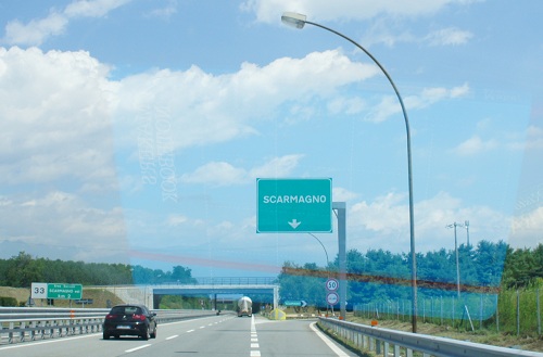
Arduino is produced in Scarmagno, a small town near the Olivetti factories on the outskirts of Turin in Italy.
All the care for the production of printed circuit boards, installation of components and distribution lies on the shoulders of this town. I was delighted with what I saw and would like to share some photos.
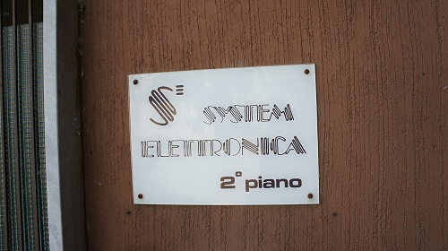
The highlight of my trip was System Elettronica, a PCB factory for Arduino.
')
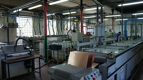
An interesting feature of System Elettronica is that the factory selected colors from the flag of Italy. In the photo of the floor you can see confirmation of this fact in the form of elements of red and white.
Arduino is born from just such huge sheets of foil textolite.
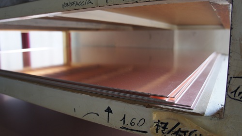
The sheets shown in the photograph have a thickness of 1.6 mm (the most common thickness for printed circuit boards, corresponding to 1/16 inch), and approximately 1 x 1.5 m in width.
The first step in the production of printed circuit boards - drilling holes. This stage of preparation takes place before applying the mask compounds for several reasons. Firstly, a mask for the connections can be set up on the existing holes. Secondly, the drilling process is dirty and sloppy, so there is a chance to damage the mask.
The photo shows the head of a CNC boring machine used for drilling holes. PCB sheets are placed in three pieces, so three holes are drilled in one pass.
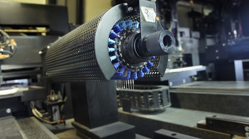
The photo shows a set of drills for the machine. If you have ever had the pleasure of messing with the creation of drilling files, you may have come across the term “drill bit set”. This is how it looks.
The video demonstrates the work of the drilling machine.
Each hole in the board is drilled by mechanics, because the number of holes affects the cost of the board. This particular machine is relatively small. I have seen huge, massive drilling tables in China, which employ between four and six drilling machines, which work dozens of panels simultaneously. The process goes so fast that the vibration is felt even at a distance of several meters.
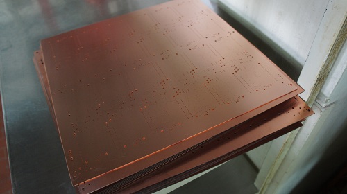
In the photo above - a PCB stack after drilling and deburring, ready for further processing.
The next step is applying photoresist on textolite and exposure. On System Elettronica, this is done using a high-contrast film. I have seen other techniques using a laser when the pattern is applied using a laser raster scan. Such methods are acceptable for rapid prototyping, but for mass production it is more practical to use film.
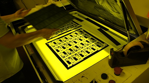
In this photo - pure textolite is placed on the svetostol for exhibiting. Please note that most of the photos are clickable so you can view them in high resolution.
The photograph shows the workpiece before and after exposure.
Then the sheets of PCB are sent for development. The same machine is used for developing photoresist and solder mask.

It looks like a sheet after development. This is one of my favorite photos.
After photo processing and development, the sheets pass through a series of baths with different solutions for the treatment of copper.
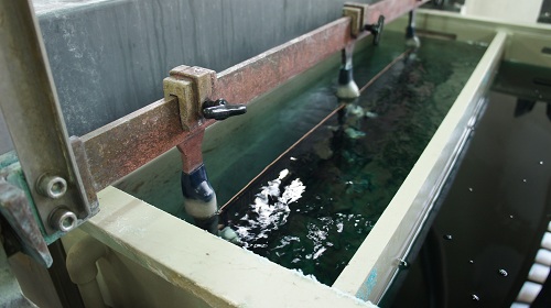
The movement of sheets in the baths is fully automated. This is necessary because oxygen can spoil the workpiece in seconds, so transportation should be as fast as possible. In addition, the baths are caustic and harmful to the human body chemicals, so it is better to let robots do it.
As you can see, the blanks gently swing back and forth. Each bath has its own solution.
After processing the blanks in solutions, a dull, white coating (I think this is nickel) is applied to all areas not covered by photoresist, including transitional and technological holes that are not covered before.

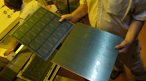
At this stage, the open and coated with a photoresist parts of copper are removed, leaving only bare PCB and protected copper.

The final stage is board surface treatment. Notice that the photos are not Arduino boards, as they were not processed on this machine when I took this photo.
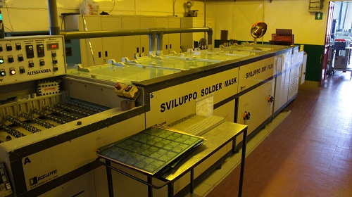
Now the boards are ready for applying the solder mask and silk-screen printing. It uses a similar process using photoresist, patterns, and developing / stripping machines.
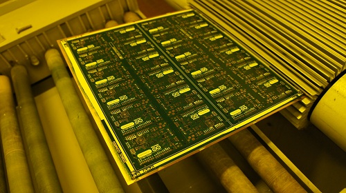
The photo shows printed circuit boards with a solder mask and silk-screen printing. In fact, silk screening is just the second layer of the solder mask. The special composition of the dry film of the white solder mask is purchased for the Arduino to achieve maximum clarity and a pleasant look that will remain even in difficult conditions of the boards. I have seen other methods of silk-screen printing, for example, high-resolution inkjet printing. This method is more suitable for the rapid production of boards. Another example of screen printing is using a squeegee and paints.
After the boards have undergone all kinds of chemical treatments, a layer of solder is applied to them using a soldering iron. After that, the boards are tested.
Each board is fully tested. This means that each track is checked for integrity and sportivivlenie two "soaring" electrodes. Such a check is a large amount of work. On the video spot above you can see how fast the process is going. An alternative to this method of testing can be the use of grab (as a shell) testers, where a set of contacts is pressed against the board to be tested. So is testing for one mechanical action. However, clamshell clamping devices are very labor-intensive in assembly and support. It is necessary after each change of connections in the project to alter the wired connections in the tester. So, in many cases, testing with “floating” electrodes can be cheaper and more flexible.
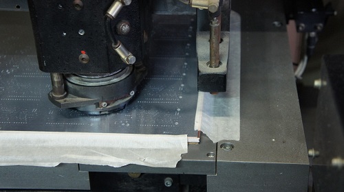
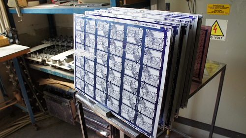
In the photo - a pack of sheets ready for the last step of slotting processing.
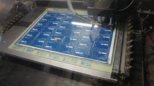
Before the boards can be sent, each sheet must be cut to fit in the machine for surface mounting. Sheets are collected in a pack and placed in the machine for cutting.
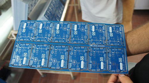
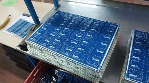
Finally, the boards are ready for soldering. As you can see, on each sheet they are arranged in 12 pieces (2x6) for maximum convenience of surface mounting.
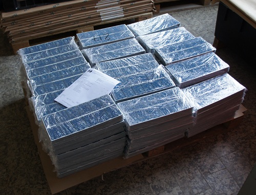
Here is a stack of about 25,000 real Arduino boards ready to leave the factory for retrofitting and selling to anyone around the world.
I express my gratitude to the Arduino team, especially Davide Gomba, for taking the time in his busy schedule, showing me everything and waiting patiently while I was photographing and in every way admiring the technique.
Arduino is produced in Scarmagno, a small town near the Olivetti factories on the outskirts of Turin in Italy.
All the care for the production of printed circuit boards, installation of components and distribution lies on the shoulders of this town. I was delighted with what I saw and would like to share some photos.
The highlight of my trip was System Elettronica, a PCB factory for Arduino.
')
An interesting feature of System Elettronica is that the factory selected colors from the flag of Italy. In the photo of the floor you can see confirmation of this fact in the form of elements of red and white.
Arduino is born from just such huge sheets of foil textolite.
The sheets shown in the photograph have a thickness of 1.6 mm (the most common thickness for printed circuit boards, corresponding to 1/16 inch), and approximately 1 x 1.5 m in width.
The first step in the production of printed circuit boards - drilling holes. This stage of preparation takes place before applying the mask compounds for several reasons. Firstly, a mask for the connections can be set up on the existing holes. Secondly, the drilling process is dirty and sloppy, so there is a chance to damage the mask.
The photo shows the head of a CNC boring machine used for drilling holes. PCB sheets are placed in three pieces, so three holes are drilled in one pass.
The photo shows a set of drills for the machine. If you have ever had the pleasure of messing with the creation of drilling files, you may have come across the term “drill bit set”. This is how it looks.
The video demonstrates the work of the drilling machine.
Each hole in the board is drilled by mechanics, because the number of holes affects the cost of the board. This particular machine is relatively small. I have seen huge, massive drilling tables in China, which employ between four and six drilling machines, which work dozens of panels simultaneously. The process goes so fast that the vibration is felt even at a distance of several meters.
In the photo above - a PCB stack after drilling and deburring, ready for further processing.
The next step is applying photoresist on textolite and exposure. On System Elettronica, this is done using a high-contrast film. I have seen other techniques using a laser when the pattern is applied using a laser raster scan. Such methods are acceptable for rapid prototyping, but for mass production it is more practical to use film.
In this photo - pure textolite is placed on the svetostol for exhibiting. Please note that most of the photos are clickable so you can view them in high resolution.
The photograph shows the workpiece before and after exposure.
Then the sheets of PCB are sent for development. The same machine is used for developing photoresist and solder mask.
It looks like a sheet after development. This is one of my favorite photos.
After photo processing and development, the sheets pass through a series of baths with different solutions for the treatment of copper.
The movement of sheets in the baths is fully automated. This is necessary because oxygen can spoil the workpiece in seconds, so transportation should be as fast as possible. In addition, the baths are caustic and harmful to the human body chemicals, so it is better to let robots do it.
As you can see, the blanks gently swing back and forth. Each bath has its own solution.
After processing the blanks in solutions, a dull, white coating (I think this is nickel) is applied to all areas not covered by photoresist, including transitional and technological holes that are not covered before.
At this stage, the open and coated with a photoresist parts of copper are removed, leaving only bare PCB and protected copper.
The final stage is board surface treatment. Notice that the photos are not Arduino boards, as they were not processed on this machine when I took this photo.
Now the boards are ready for applying the solder mask and silk-screen printing. It uses a similar process using photoresist, patterns, and developing / stripping machines.
The photo shows printed circuit boards with a solder mask and silk-screen printing. In fact, silk screening is just the second layer of the solder mask. The special composition of the dry film of the white solder mask is purchased for the Arduino to achieve maximum clarity and a pleasant look that will remain even in difficult conditions of the boards. I have seen other methods of silk-screen printing, for example, high-resolution inkjet printing. This method is more suitable for the rapid production of boards. Another example of screen printing is using a squeegee and paints.
After the boards have undergone all kinds of chemical treatments, a layer of solder is applied to them using a soldering iron. After that, the boards are tested.
Each board is fully tested. This means that each track is checked for integrity and sportivivlenie two "soaring" electrodes. Such a check is a large amount of work. On the video spot above you can see how fast the process is going. An alternative to this method of testing can be the use of grab (as a shell) testers, where a set of contacts is pressed against the board to be tested. So is testing for one mechanical action. However, clamshell clamping devices are very labor-intensive in assembly and support. It is necessary after each change of connections in the project to alter the wired connections in the tester. So, in many cases, testing with “floating” electrodes can be cheaper and more flexible.
In the photo - a pack of sheets ready for the last step of slotting processing.
Before the boards can be sent, each sheet must be cut to fit in the machine for surface mounting. Sheets are collected in a pack and placed in the machine for cutting.
Finally, the boards are ready for soldering. As you can see, on each sheet they are arranged in 12 pieces (2x6) for maximum convenience of surface mounting.
Here is a stack of about 25,000 real Arduino boards ready to leave the factory for retrofitting and selling to anyone around the world.
I express my gratitude to the Arduino team, especially Davide Gomba, for taking the time in his busy schedule, showing me everything and waiting patiently while I was photographing and in every way admiring the technique.
Source: https://habr.com/ru/post/149855/
All Articles