Visualization of the board made in EAGLE using Photoshop
Unsubscribe how to visualize a printed circuit board designed in CAD EAGLE using Photoshop. But I want to warn you right away that this method does not take into account the presence of interboard transitions (vias) and surface-mounted sites (smd).
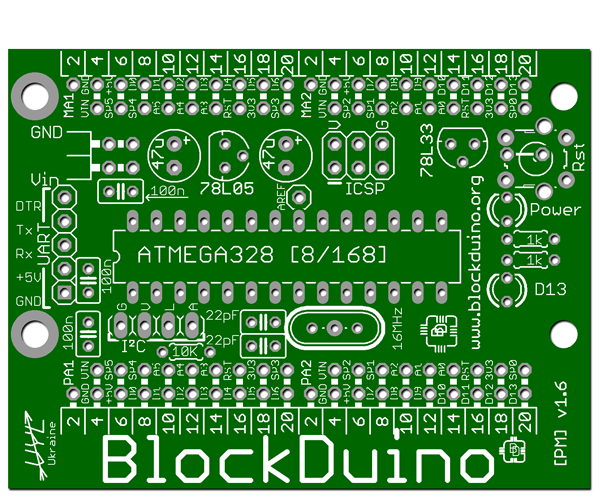
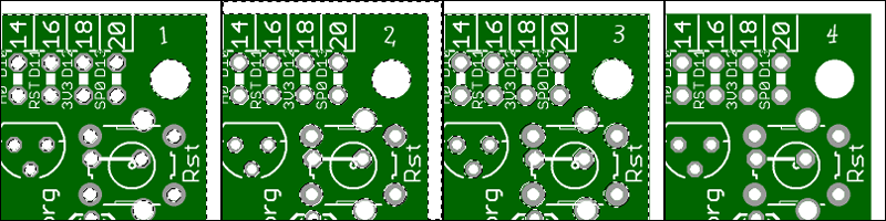
At the exit:
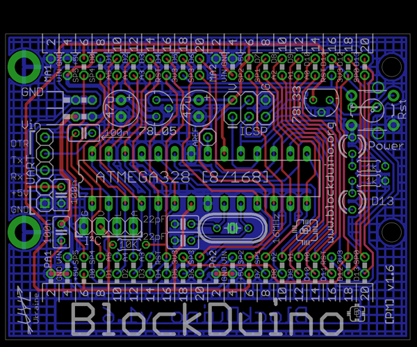
At the entrance:
For this you need: a board file (with the extension .pcb), the EAGLE program, and of course Photoshop.
')
In EAGLE, select the 'tPlace', 'tNames' and 'tValues' layers. And everything is as usual: export, create a mask, fill it with white color, call it 'Silk'. Upd: When creating a mask, you need to change the 'Tolerance' to 64.
In principle, at this stage you can stop, the board already looks like:
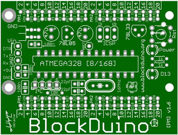
But, as you can see, the markings on the board crawl onto the platforms. In a real board, all this will be cut off at the preparation stage, we will do the same:
To give even greater likelihood you need to add a bit of volume. To do this, make the 'PCB' layer cast a shadow. This is done using the 'Styles' dialog box. You can also create a layer 'Top' - the top tracks. But this is already as a homework.
Keep, study, analyze, show off.
By the way, I often noticed blots on the board at this stage, especially in the marking layer.
Well, at the end for comparison, what I visualized as much as possible, and what happened in real life (the previous version of the board was scanned).

At the exit:
At the entrance:
For this you need: a board file (with the extension .pcb), the EAGLE program, and of course Photoshop.
')
Step 1 - Create a Virtual Board: Preparation and Dimension Layer
- Open the board in the EAGLE, remove all layers except Dimension
- We export as a picture to the clipboard: choose File-> Export-> Image, set the Clipboard checkbox, change the extension to 600 (for good quality) and click Ok.
- Open Photoshop, create a new document (File-> New, or press [Ctrl-N]). In the dialog box:
- call the document
- make sure that the Preset is Clipboard (otherwise we have empty clipboard)
- Change Color Mode to RGB
- click Ok
- Paste the clipboard into the image (Edit-> Paste, or [Ctrl-V])
- Create a mask for the layer:
- Select the tool 'Magic Wand Tool', set the Tolerance - 0, and put a tick on the Contiguous
- Click in the center of the board
- Click on the button 'Add layer mask' under the list of layers
- We paint the board:
- Click on 'Layer thumbnail' choosing the layer itself, not its mask.
- Fill with color: 'Edit-> Fill ..', select 'Use: Color', and select the desired color, for example # 006600 (R-0, G-123, B-0), click 'Ok'.
- Change layer name to 'PCB'
Step 2 - Create contact pads and drill a virtual board
- Go to EAGLE, select only two layers - Pads and Vias. We export (File-> Export-> Image-> Ok).
- Go to Photoshop and paste the picture (Ctrl-V).
- Create a mask for the layer:
- select the 'Magic Wand Tool', you can use the [W] button,
- uncheck the Contiguous and click on the pad
- click on the button 'Add layer mask' below the list of layers
- Click on 'Layer thumbnail' and paint over with gray, for example # 999999 (R-153, G-153, B-153)
- Put a tick on Contiguous and on 'Sample All Layers', click in the middle of the board (not on the pads)
- Next, remove the tick on 'Contiguous' and hold down the Shift key, click on the contact area (adding a selection)
- Invert the selection 'Select-> Inverse' or [Shift-Ctrl-I] and delete the excess: select 'Layer mask thumbnail' on the 'PCB' layer and fill it with black.

Step 3 - Marking
In EAGLE, select the 'tPlace', 'tNames' and 'tValues' layers. And everything is as usual: export, create a mask, fill it with white color, call it 'Silk'. Upd: When creating a mask, you need to change the 'Tolerance' to 64.
In principle, at this stage you can stop, the board already looks like:
But, as you can see, the markings on the board crawl onto the platforms. In a real board, all this will be cut off at the preparation stage, we will do the same:
- right-click on the 'Layer mask thumbnail' of the 'PCB' layer and select the 'Add Layer Mask To Selection' option
- Invert the selection 'Select-> Inverse' and add a selection from the 'Pads' layer
- For greater likelihood, slightly expand the selection: 'Select-> Modify-> Expand-> 2pixels-> Ok'
- Left on the 'Layer mask thumbnail' of the 'Silk' layer and fill it with black.
Step 4 - Final - Finishing
To give even greater likelihood you need to add a bit of volume. To do this, make the 'PCB' layer cast a shadow. This is done using the 'Styles' dialog box. You can also create a layer 'Top' - the top tracks. But this is already as a homework.
Keep, study, analyze, show off.
By the way, I often noticed blots on the board at this stage, especially in the marking layer.
Well, at the end for comparison, what I visualized as much as possible, and what happened in real life (the previous version of the board was scanned).
Source: https://habr.com/ru/post/149026/
All Articles