About the power interchange with examples
 When I participated in the 7400 contest , I realized that many of the presented logic circuits for reliable operation lack the simplest security features. One of the most common design flaws was the lack of blocking tanks. Later, after reading an article on Murphy's law , I decided to write a little about decoupling and blocking capacitors.
As a person who can be called an old-timer in the field of electronics, I became acquainted with the problem of lack of isolation from my own experience. I collected my first high-speed circuit as an intern at a major electronics company. That scheme, a digital frequency meter, was assembled on the logic of the 74Fxx family and operated at a frequency of 11 MHz (at that time it was considered very much). It was a 23 × 16 cm board (Double Eurocard ) containing about 40 microcircuits connected by wire wrap . When it came time to turn it on, I saw that the circuit was not working as it should, but it gave out complete nonsense.
After checking the assembly several times, I told my manager about the problem, and he glanced at the board and said: “There are not enough blocking capacitors. Put them on food near each microcircuit, then we'll talk. ”Completely confused, I did, as was said, and - lo and behold! - it all worked right away. Why the seemingly unimportant capacity made the circuit work? My supervisor told me about the surge current when switching, the inductance of the conductors and the decoupling. I admit that several years passed before I really understood what he was saying then, but the lesson was learned: always to put capacitors on the power of digital microcircuits.
The terms “blocking capacitor” and “decoupling” are not random words, but have a definite meaning in this context:
decoupling is an action aimed at (partial) separation of the power supply circuits of the microcircuit from the common power source;
blocking capacitor - a capacitor installed in such a way that it shunts the power supply to the microchip and acts as a local power source.
')
Why is this all so important? Look, for example, here:
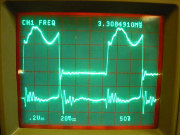
Figure 1. No blocking capacitors.
Does it look like a digital signal? This nonsense you get without blocking capacitors.
Please note that the clock frequency is not important . The problem lies in the rising and falling edges of the signal. So, the same considerations apply to systems operating at 1 Hz, 20 kHz or 50 MHz. The frequencies used in the examples below are chosen so that they can be conveniently observed on an oscilloscope.
It should be noted that at high frequency failure occurs faster than at low, due to a larger number of fronts per unit time. However, this does not mean that low-frequency circuits will work reliably. Far from it, they will fail just as easily, according to Murphy's law. Oh, and by the way, have you thought about your small microcontrollers operating at 16 MHz?
Current Surge Measurement
To see what is happening, you need to measure the currents flowing through the circuit. Here is a simple experimental setup assembled for illustration: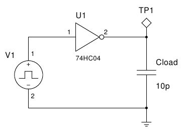
Figure 2. Connecting the inverter.
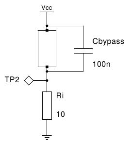
Figure 3. Measuring circuit.
The pulse generator is connected to an inverter 74HC04, loaded on a capacitor of 10 pF. The signal at the inverter output, TP1, is shown in the upper waveform. The power source is connected to the terminals of the microcircuit 7 and 14. In the gap of the earth conductor a current-measuring resistor 10 Ohm is included.
The voltage at TP2 is proportional to the current consumed by the chip and is displayed on the lower oscillogram. The blocking capacitor can be connected or disconnected if necessary. The oscilloscope probes are equipped with 1:10 dividers, so the vertical scale of the oscillogram must be multiplied by 10. All unused inputs 74HC04 are grounded. The installation looks like this:
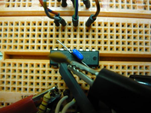
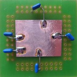
Figure 4. Installation assembled on a breadboard.
Figure 5 shows problems at high and low frequencies. Pictures on the left - without a blocking capacitor, on the right - with him.
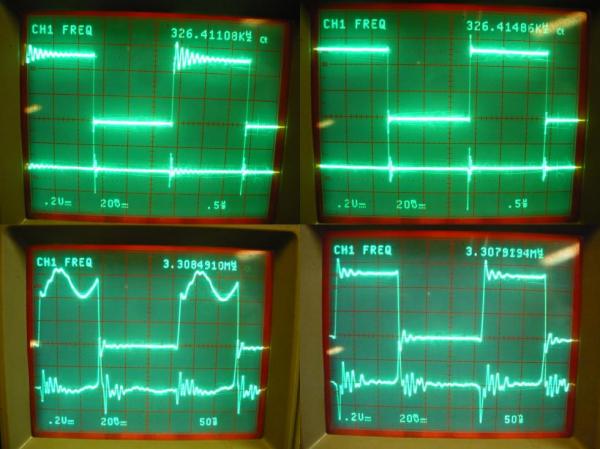
Figure 5. Output voltage (upper channel) and current consumption (lower channel).
Above - the clock frequency of 330 kHz, below - 3.3 MHz.
On the left - without a blocking capacitor, on the right - with it.
Some observations from Figure 5:
- The measured current is only the current through the GND foot and the blocking capacitor. It does not exactly match the current consumed by the chip. It is difficult to measure the current through the legs of Vcc and GND at the same time (limitations imposed by the design of the oscilloscope. - Appro. Transl. ) . However, measuring current through a GND pin is sufficient for illustrative purposes.
- With a logical “1”, a high-frequency “ringing” is observed at the output. Its span is greater than 2 V, and emissions exceed the supply voltage. Adding a blocking capacitor reduces the “jingle” to an almost insignificant level. Emission still remains, but decays much faster.
- The signal fronts correspond to outliers (“needles”) of the current consumed. Adding a blocking capacitor reduces these outliers and makes them symmetrical with up and down fronts. The emission range is from -22 to +45 mA without a blocking capacitor and from -32 to +36 mA with it.
- The symmetrical form of the current in the presence of a blocking capacitor says that energy is stored and removed back. This is a very important feature.
- The residual HF ring largely depends on the position of the oscilloscope probe (not shown), which suggests that the circuit contains spurious LC elements and radio frequency antennas. The location on the board and the relative position of the connecting wires have a significant effect on the amplitude and frequency of oscillations. This interference can not be completely eliminated, but it can be greatly reduced by properly spreading the printed circuit board.
Take a closer look at the signal fronts:
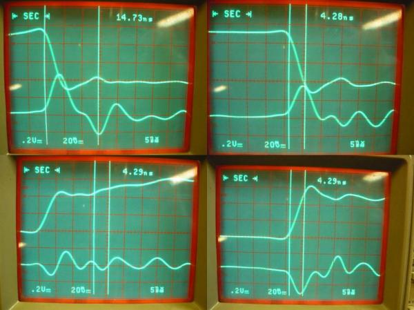
Figure 6. Output voltage fronts (upper channel) and current consumption (lower channel).
From above - the back (falling) front, from below - the front (rising) front.
On the left - without a blocking capacitor, on the right - with it.
Current consumption estimate
The 74HC04 chip is made using CMOS technology. This means that the static current consumption is close to zero. The current is consumed only when switching from "0" to "1" and from "1" to "0". When switching all load and stray capacitances must be reloaded. For the experimental circuit, the load has a capacity of 10 pF. Here you need to add the capacitance of the conclusions and parasitic capacitances, which are approximately 5 + 2 pF. The oscilloscope probe has a capacity of 10 pF, which must also be taken into account. Thus, the total load capacitance at the output of the inverter is approximately 27 pF.The output capacitance needs to be charged from 0 to 5 V in about 4.3 ns. Taking for simplicity that the charging current is constant, we estimate its value:
Q = I · t = C · U
I = (5 · 27 · 10 -12 ) / (4.3 · 10 -9 ) = 31.4 mA
This means that a huge current (by the CMOS standards. - Appro. Transl. ) Current flows in or out through the inverter output at each switch. Where does the energy come from? Of course, from the power source. Figure 6 clearly shows that the current does not occur instantaneously, but rises to a certain level, and then drops again. This behavior clearly indicates the presence of inductive elements.
This is best seen in Figure 6 on the right, where the current reaches a maximum at the moment when the output voltage drops to zero. The current then drops, causing the output voltage to dip. The calculated current coincides quite well with the measured, given that only the simplest estimate was made.
So why do you need a blocking capacitor?
Once again, take a close look at the lower half of Figure 6. On the left, the output voltage does not reach 5 V for some time, and on the right, it reaches almost immediately. Without a blocking capacitor, the microcircuit lacks the power supply to form a steep front, and the voltage is stuck at 4 volts. The blocking capacitor provides the necessary instantaneous power for a while.The blocking capacitor is about 4000 times larger than the load capacitance, which means that it should be expected that the supply voltage drop will be 4000 times lower (than the output voltage swing. - Approx. Transl. ) - about 1-2 mV.
When switching back from “1” to “0”, as in Figure 6 above, the blocking capacitor acts as a reservoir for receiving the released energy. The load capacity is discharged and the current must flow to the ground. However, the energy cannot be instantaneously transferred to the power source, and the blocking capacitor will temporarily store it.
Local power supply
The main power supply cannot provide the chip with sufficient power due to the inductance of the conductors. Each wire has a parasitic inductance, which prevents the change in current. From the definition of inductance:U = L · dI / dt ⇒ dI = U · dt / L
From this equation it can be seen that the change in current is inversely proportional to the inductance. In other words, if the inductance increases, it becomes more difficult to change the current for a given period of time, all other parameters being equal. In addition, a change in current causes a voltage drop across the inductance. The longer the wire (or track on the board), the higher the inductance it has, the more it resists the rapid change in current, and the greater the voltage drop.
The blocking capacitor is a local energy storage. It should always be installed as close as possible to the power supply pins of the microchip to minimize the inductance of the conductors from the capacitor to the microcircuit. Such a scheme unleashes the common and local supply chains.
Increase the load
The microcircuit consists of six inverters, so the circuit can be changed so as to increase the current consumption:
Figure 7. Experimental scheme with additional load.
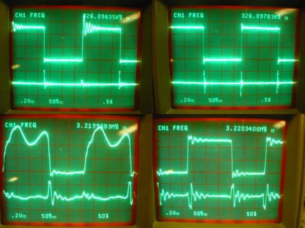
Figure 8. Output voltage (upper channel) and current consumption (lower channel) for the circuit with additional load.
Above - the clock frequency of 330 kHz, below - 3.3 MHz.
On the left - without a blocking capacitor, on the right - with it.
Note the different scale along the Y axis for the current measurement channel, compared to Figures 5 and 6.
The current through the GND pin now has emissions of about 70 mA in the absence of a blocking capacitor. If the latter is installed, we again observe a symmetrical form of emissions with an amplitude of ± 50 mA with rising and falling fronts.
Notice that the signal front, as seen in Figure 8 below left, is now much more gentle. The microcircuit simply does not have enough energy to switch quickly. Installing a blocking capacitor (figure 8 on the right) restores the steepness of the front to an acceptable level.
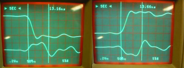
Figure 9. Output voltage fronts (upper channel) and current consumption (lower channel).
Left - the rear (falling) front, on the right - the front (rising) front.
Interlock capacitor installed.
A detailed examination of the signal fronts reveals an increase in duration of the current surge, which is caused by the large energy requirements. The chip load is about six times higher than before (the first inverter is loaded on the input capacitances of the remaining inverters, which are 5 times 5 pF).
It was just a simple example - a microchip of six inverters. And now extrapolate the above to a complex logic circuit containing many elements and many internal connections. It has a lot of parasitic capacitances, which must be recharged each time the input signals change. Finally, imagine a microcontroller consisting of many thousands of gates.
Grounding
The above explanations and illustrations should give a clear understanding that the blocking capacitor is an important element that performs its special function. It stores the energy of the power source locally, gives it out if necessary, and also accepts excess energy.Local energy storage is constantly replenished from the main power source via the Vcc conductor. At the same time, the excess energy must be discharged to the power supply through the GND conductor. The discharge of energy into the blocking capacitor increases the voltage on it, and, in fact, briefly creates a local area on the circuit with a different potential. The elimination of this imbalance is very important and is carried out by grounding. (Here, grounding is not a connection to the mass of our planet, but a connection to the common wire of the power source. - Appro. Transl. )
Printed circuit boards often have separate grounded layers, which are very effective for connecting elements with a common power supply conductor. Well-designed wiring of the earth is of paramount importance for the discharge of excess energy. But be careful, eddy currents can occur in a solid grounded layer, and numerous connections with a common wire can form a so-called. ground loops.
It will always be a good idea to contact a familiar developer with experience. Most mistakes have already been made before by anyone, and there is no need to repeat them ad infinitum.
Source: https://habr.com/ru/post/146987/
All Articles