A critical view from the side on processors Multiklet / Multiclet
 In the past couple of weeks, on many sites there were notes about the start of production (at Asian factories) of domestic Multiclet processors with “breakthrough architecture and fantastic performance”, including on Habré: The first pilot batch of domestic multicellular processors MCp . All of these notes generally looked at the development from the positive side, based on the advantages presented by the developers. I have always been interested in domestic developments, and I will try to tell a little more critically about this processor and describe the essence of this new architecture to the best of my abilities.
Sources of information - limited documentation available on the developer's site, and answers to questions by company employees.
Architecture
If we discard all the verbal husk (and there is especially a lot of it in this case), the multi-clet is in its first approximation the EPIC favorite in Russia and the USSR: architecture with explicit parallelism. Unlike VLIW, where the compiler indicates which block should do what, only the dependencies of the instructions are indicated, and they are taken apart in the process of execution (there are 4 such cores in MCp0411100101 ).
')
Abroad, this architecture is known, and since 2006 it has been working in silicon ( Explicit Data Graph Execution / TRIPS ), but no massive commercial success over the past 6 years has been seen.
Advantages compared with VLIW here 2: a hypothetical possibility to run the code on a processor with a different number of "cores" and the ability to continue work when one of the cores fails. Both advantages, in my opinion, are very doubtful:
1) Running without recompilation on a larger processor - for embedded applications there is usually no problem in recompiling. In addition, the optimal code for 4 and 16 cores is different - and running without recompilation reduces efficiency (of course, if we do something harder than multiplying arrays).
2) Resistance to failure of any core - this "chip" appeared recently.
According to the latest information, there is no stability in the released chip; it may appear in the future with the necessary changes.
Now let's look at the picture from the processor description (PP - program memory, PD - data memory, PB - processor unit):
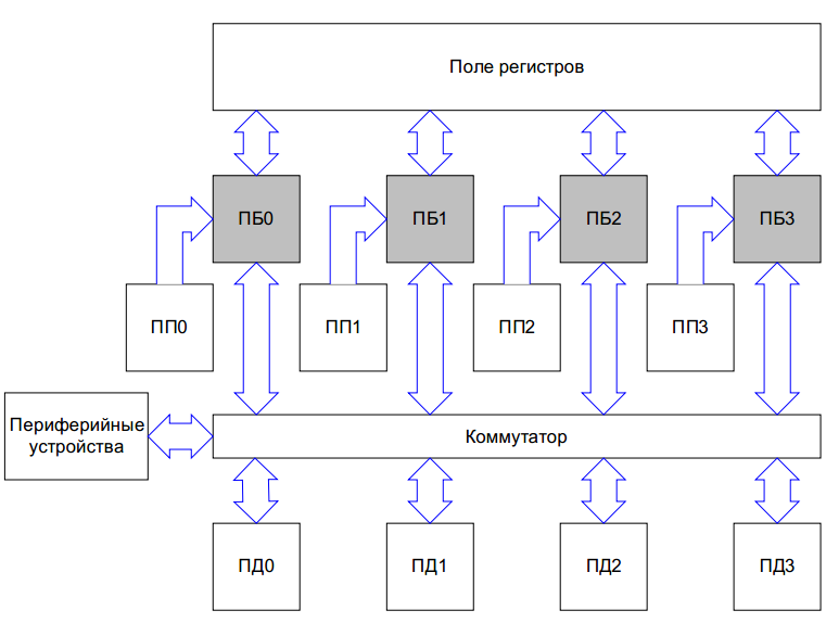
Immediately struck - a common register file and a switch, shared access to memory (when all the cores can read and write almost anything). Typically, this kind of architecture works slowly (due to purely physical limitations), and perhaps this is the reason why the Multiklet works only at 100 MHz when manufactured at a foreign factory (
It is precisely because of speed problems that all other existing (commercially successful) multi-core architectures do not attempt to organize access “everyone has access everywhere” - usually the kernels have small local memory with the possibility of rare slow access to shared memory.
Performance
It would seem that 2.4GFLOP declared by the manufacturer is a very significant performance. However, the processor company declined to explain how such performance was obtained at a clock frequency of 100 MHz, and did not confirm that madd (multiply + add) runs in 1 clock cycle. Nevertheless, it seems that I managed to understand where this figure came from.
The multiclet works with single precision numbers - “single” (32-bit) and it is possible to pack a complex 64-bit single-precision number (ie, the real and imaginary part of 32 bits). Then it turns out that if the multiplication of two complex numbers is performed in 1 clock cycle, then it gives 6 FLOP per clock: (a + bi) (c + di) = (a + bd) + (ad + bc) i., And accordingly , 6 * 4 * 100Mhz = 2.4GLOP.
Thus, it’s impossible to compare this performance with desktop Pentium s (you like to do this in the discussion: “almost got Intel”): in desktop processors, it’s customary to measure productivity on 64-bit real numbers, and here the performance figures sounded only 32-bit and only in specific conditions.
In normal operations with unpacked data, the performance is 400 million operations per second, and you need to keep in mind that the instruction set here is much simpler than in the same armam, i.e. the speed on ordinary tasks will be lower than that of the 400Mhz arma (or Komdiva-64 ).
Those. in fact, the new Multiklet architecture turned out to be “heavy”, and it works with such a small clock frequency that the single-core processors of the classical architecture turn out to be faster in the end.
power usage
Unfortunately, there is nothing to discuss here, it needs to be carefully tested on a real load and a real chip. If there is a visible advantage in terms of energy consumption, then it is possible for some tasks that will be a selection criterion.
Peripherals and other stuffing
First, we pay attention to the amount of memory - 16kb of program and data memory each.
There is no external memory controller, so all the talk about porting Linux is a matter of a distant and foggy future, before which you still have to make a backend to GNUC for this processor.
There is no flash memory for storing the program, and the download is made from an external USB flash drive (currently Xilinx XCF04S). Naturally, this aroused suspicions that the processor was remarked FPGA, but my direct question about this was answered to me:
Instead of Xilinx, you could put any flash drive, and the crystal is a crystal (look carefully at the site), we are not doing anything on the FPGA. They did it at the OCD stage to confirm the calculated parameters.The crystal is made over 180nm.
The periphery is more or less understandable for those who worked with microcontrollers, with the exception of Ethernet and USB - there is no “physical” part of the interface on the chip, and they need to be put on board with separate microcircuits.
Software for development - at the moment only assembler. Compiler C is in the “bubble sorting” stage (Update: and factorials). A detailed description of the architecture required for developers is not available at the moment.
Summary
The architecture of the Multiklet is,
The achieved practical performance of the first processor of 400 million operations per second is comparable, and sometimes even less than the performance of serial single-core processors of the classical architecture produced in Russia (I’m not talking about foreign processors and DSP, of course) due to a higher clock frequency and more “meaty” set instructions last.
A further increase in productivity _in my view_ promises to be difficult, because the more cores we place on a chip, the slower each core will work due to the fact that the overhead of maintaining the “all cores have access everywhere” scheme quickly grows with the number of cores.
The declared “stability” of the processor to failures is a matter of a foggy future, now it is not there.
Proceeding from all this, I do not think that this “fundamentally new (post-Neumann) multicellular architecture” is a breakthrough in processor engineering.
It works - yes. Better than competitors (including Russian ones) - hardly.
I will be glad to hear your additions and corrections - the available information on Multiklet is very limited, and I may well be mistaken somewhere.
Update: Updated data on the accuracy of real numbers, 24-> 32bit, 48bit removed, rewritten in light of this summary in a more positive way.
Update: More clearly separated their speculation from the facts.
Update: Thanks to beeruser , we discovered that this architecture ( Explicit Data Graph Execution / TRIPS ) has been known in the West for a long time, and you cannot call it new. Because they ALREADY didn’t take off from them, the probability of taking off from us is extremely small.
Update: Supplements from developers have been received - the crystal is made at 180nm, fault tolerance is not in the current processor, it may appear in the future.
Source: https://habr.com/ru/post/146964/
All Articles