Self-assembled 3D structures for nanoelectronics
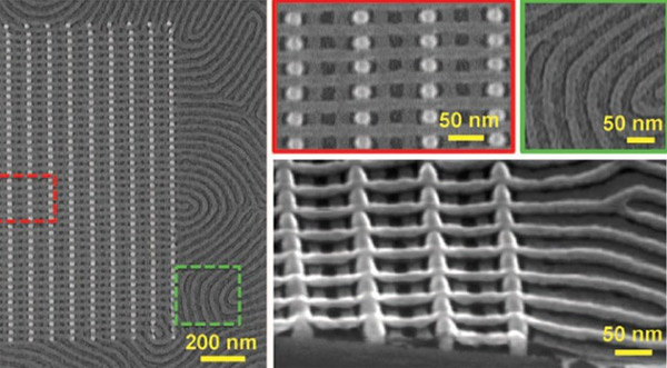
MIT engineers invented a new method of self-assembly of wires 15 nm thick on a silicon substrate coated with polymer. The thickness of 15 nm is more than two times smaller than the size of the components in the smallest modern chips. Thus, the road is open for further miniaturization of microcircuits.
Although the wires of 15 nm were obtained in other experiments, the engineers from MIT for the first time managed to design a 3D structure in several layers (in two).
')
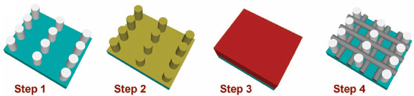
A phased process of self-assembly of wires is shown in the illustration and in the video. On a silicon substrate, an electron lithography technique creates a grid of miniature columns 10 nm thick. It is possible to do this even on serial equipment for e-lithography, which is installed in the factories of Intel, TSMC and other companies.
They are covered with a block copolymer, which by its properties tends to curl into long cylindrical structures. By accurately calculating the distance between the columns, you can pre-program the block co-polymer to create wires of the required shape and thickness, as well as pave the route for them on the surface of the chip. The bars set the properties not for one, but for two layers of wires, which allows you to create complex 3D configurations. In the future, you can try to go to the three-layer configuration, while maintaining full control over the structure of each layer.
This is a very important technology for creating electronic microcircuits of submicron size. Researchers from MIT say that within a year they intend to create the first efficient electronic device.
Source: https://habr.com/ru/post/145961/
All Articles