Making Chips at Home - Step 2
 Since the publication of the first article on my home chip project, a year has passed (rather flew by), it’s time to share progress and new problems.
The original goal of the project is to learn how to make chips in the home, consisting of hundreds / thousands of transistors (level KR580VM80A / Z80).
Due to the fact that the project turned out to be quite large for the required resources and time - I decided to get as an additional result - a documented, as simple as an open-source process technology, which allows you to create chips in limited conditions. In the United States, perhaps this would be a good reason for the project on the kickstarter, but apparently not destiny.
')
About solving complex problems and human limitations
For the first six months, the task ahead of me sometimes seemed simply unaffordable. Not everything is clear everywhere; the list of things that need to be done or which need to be dealt with was endless. Only later did I understand the basic principle of solving complex problems:
Man - in principle, not able to solve complex problems. All that he can do is make one next simple and obvious step along the long staircase leading to the solution of the problem. If the problem is not obvious to solve it in one step, all that remains is to study and break it down into subtasks until it becomes obvious. After that, in the worst case, it turns into a logistical problem - the problem of managing a large number of simple subtasks.
This is exactly what happened, as we studied and worked out - the task became logistic, and it came down to finding all the necessary components and choosing from the known options for solving each technological problem based on the existing limitations in terms of size, finance and security.
About technological solutions
- Technical process - NMOS (or PMOS as a last resort), with one type of transistor and one doping. How it all works and is designed - it is clear. CMOS is rather complicated for diffusion doping, and leave it for later.
- From compressed gases - there will be only Argon for high-temperature annealing and spraying of metals. But I will try to do without it - hydrogen / nitrogen.
- Oxygen (for growing an oxide layer on silicon) and hydrogen (for annealing) will be obtained by electrolysis of water on nickel electrodes in an alkaline electrolyte. Slight alkali metal contamination should not be a big problem. I think it is clear that I would not want to carry oxygen cylinders and especially hydrogen to take home.
- There will be no epitaxial layers (i.e., growing a layer of silicon), since monosilane (the gas from which the silicon layer is growing) is too dangerous for the house due to its explosiveness, and getting it “in place” in microscopic quantities will not come out. Accordingly, the transistors will be with a metal gate, i.e. relatively slow.
- Photolithography - all my old and naive thoughts about quartz optics, hard 253 / 184nm UV - go to the landfill. There will be standard lenses and 365 / 405nm near-UV light. This removes the issues with relatively exotic photoresists.
- Sputtering metals in vacuum - plasma, rather than heating in a tungsten boat. It is much simpler and more flexible, does not require the actual boats and the sophisticated electronics of heating and temperature control. Metal - aluminum. I know about the desired 1% alloy with silicon, but so far I don’t know exactly what I’ll do with it. The puncture of the pn junction due to the use of pure aluminum can be avoided in different ways, and electromigration is not a significant problem for this task.
- The stove is a banal nichrome on a quartz tube. Temperature control - by changing the resistance of Nichrome or, in the worst case, by the power output per spiral (i.e., blindly). I bought the high-temperature thermocouples - but they are too big for my ultra-compact dimensions.
- The photoresist is a banal novolac photoresist with an alkaline developer. Again, alkali metal contamination is not fatal for the initial task, so with the expensive metal-free developers (based on TMAH ), I decided not to bother.
Promotion by materials
In addition to the dull silicon wafers - silicon on sapphire (in production - used for radiation-resistant microcircuits). In my case, the technical process in some steps can be simplified:
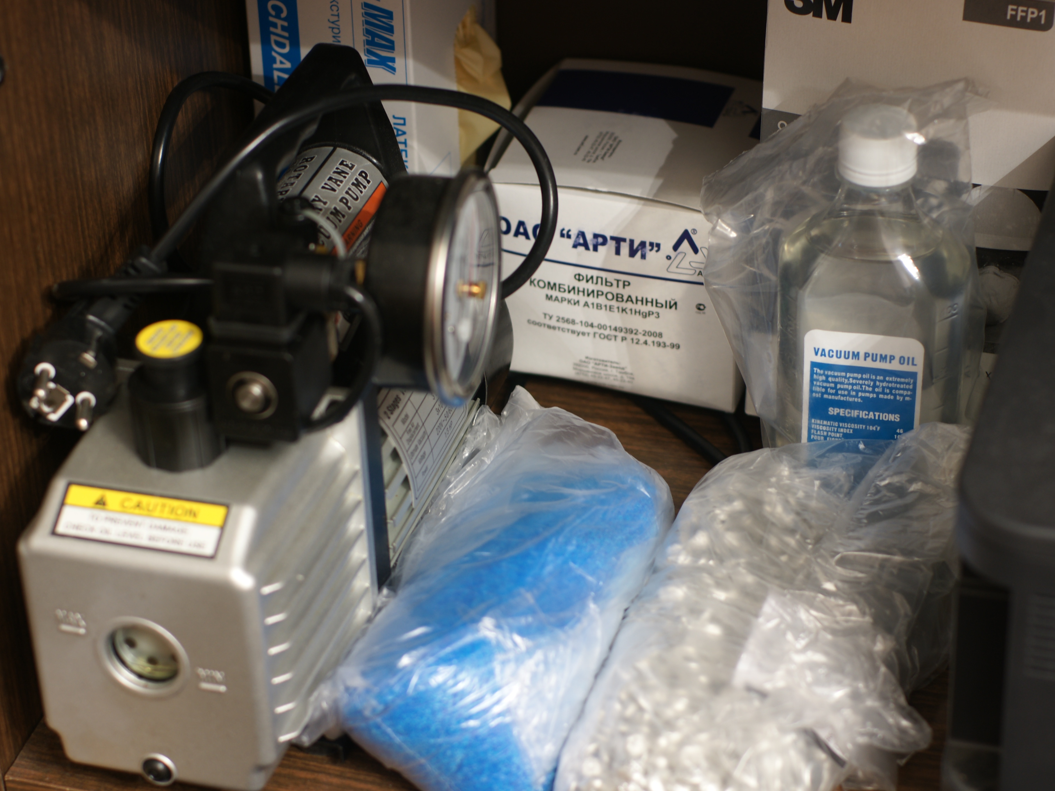
A two-stage vacuum pump with fittings (electric faucets, vacuum hoses, pressure gauges, etc.) arrived from China - it should be enough to spray metals:
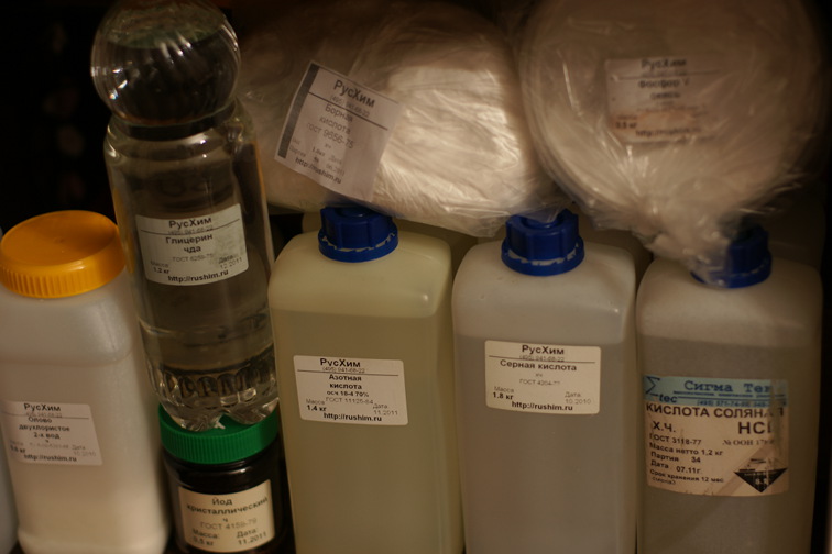
Acids - sulfuric, hydrochloric, nitric, boric, orthophosphoric ... Many are concerned about the precursors and the state drug control - I have everything acquired legally, with the passage of the relevant bureaucratic procedures.
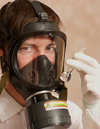
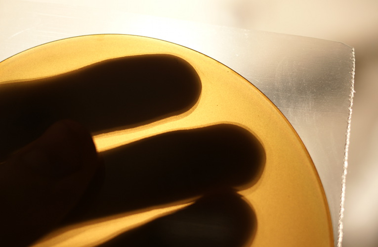
 And overseas, fluoride. This is my biggest mistake in life. The store refused to spill (because of its danger), and said that they could only sell the whole, 24kg. Then I did not see other options, and agreed. But I was really afraid of her - after a long time I watched a video about working with hydrofluoric acid - then I had a nightmare that I poisoned her, there is no antidote and that’s the end (not far from the truth, the topic was revealed in the 20th series 4 season ER / Ambulance ). The idea was “brilliant” - to hell with it, I will spill it myself and sell the extra. But after the first 2 kilograms, which had to be poured by a 20-cubic syringe, in a gas mask, etc., when at my feet defiantly sizzles concrete, dissolving in the places where I spilled a couple of drops - I decided - well, what for him. It turned out a kind of suitcase without a handle, which is not just a pity to throw out - it is impossible, because damn dangerous.
As a result, I presented this suitcase to the seller with chemistry by self-delivery, keeping the minimum required amount for myself. It was a good lesson.
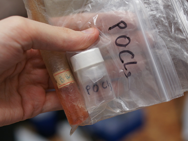
After that, the most dangerous substances in the production of microcircuits that I have to use are sources of phosphorus and boron for doping: BBr3 and POCl3 - I bought them with the most minimum necessary volume. There are safer alternatives - the so-called spin-on dopants - but manufacturers do not want to sell it to me, due to liability issues. If it does not come out with the process in the old manner, I will finish the manufacturers.
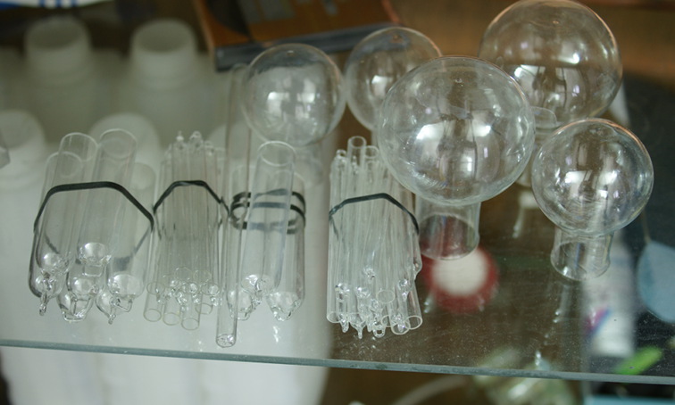
Quartz utensils for micro stoves up to 1000C
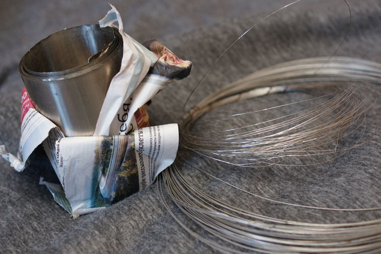
Nichrome wire (diameter 0.4 and 0.8mm), nickel rolled for electrolyzer electrodes:
Industrial photoresist for microelectronic applications. I decided not to chase the resist with the thinnest possible, this one is quite oak 2 micron. Thicker layer - easier to work on, at the beginning it should be enough. While there is no adhesion promoter ( HMDS ) - it was not available, I will try without it:
 As noted by some people who helped me with advice, it is possible to make chips only in the laboratory. You can make them at home only if at home - a laboratory. It seems to be the case
 In general, the most necessary things in logistics are already there.
There are things to which the toad does not let me in yet:
- A metallographic microscope - in Russia, Chinese microscopes are resold by 100-300 thousand rubles, in the homeland of elephants they are 1500 $ -3000 $. This is probably also a necessary thing, so far I can not only find Chinese who would sell it to me with Escrow.
- Laboratory Nitrogen Generator - hotties sly stuff. Nitrogen gets from the air, consumables are not. You could make an oxygen-free box with him and remove the inert gas problem. But it costs about 190 thousand rubles. I will do without him.
- The generator of deionized water is also a useful thing in the household, but it is very simple for ~ 45 thousand rubles. I will try to “collective farm” my own on ion-exchange resins (only out of interest, it is clear that DI can buy water)
Remaining problems and what i'm looking for
- Detailed descriptions of (old) technical processes with specific numbers. I found one, and he helped me a lot, but it would be extremely useful to look at another 1-2.
- "Open" (i.e., when the contents of standard cells are directly visible in layers) digital libraries for relatively thick technical processes
- I am looking for someone who can help set up software for designing chips and tell how anything is there - to have a general idea, and I could synthesize simple test circuits. It is clear that I can draw a shift register on a piece of paper, but something a little more complicated ...
- We have not yet succeeded in buying vacuum tires for a metal spraying chamber.
- I will also slowly search for where to buy spin-on dopants and spin-on glass samples for ILD (a dielectric that separates the levels of metal wiring).
- Small volumes of TMAH , HMDS and TEOS .
Feel free to email me if you have thoughts about solving these problems.
Further steps
In general, there is still a long way ahead, but it is no longer covered with fog, as before. Now that the main components are already in place, the creation of electronic control units for the heat of the stove with temperature control (or even an automatic oxide thickness calculator) and an electrolytic cell with the separation and drying of hydrogen and oxygen are ahead.
I should note that without the help of people (both information / advice and materials) that responded to the previous article - my progress would have been much more modest.
Yes, and once again about the most beaten question - “why all this” for me personally and in general: I do this because I find it interesting, a kind of hobby. On the other hand, work on this project has already allowed me to understand how the "big" microelectronics works (from a technological and financial point of view). In addition to this - now I am working on a "classic" microelectronic project, which (if everything goes according to plan) will be implemented in high-volume production: a general-purpose microcontroller - but more on that another time.
Questions / tips / comments?
Source: https://habr.com/ru/post/145373/
All Articles