An inside look: Plastic Logic

On Monday, May 14, at the Moscow office of RosNano, the first of the three (held in Moscow, Dresden, and Cambridge) was held by PlasticLogic's TechOpenDay . Due to the abundance of materials ( 1 , 2 , 3 ) dedicated to this event and describing it, in my opinion, a little superficially, let us try to figure out what was presented to the public a couple of days ago.
How did I get to this event?
Quite by chance, on the working Saturday, the main character of the video about the prepreg called me and offered to attend the event. Honestly, at first I was wary of such an invitation, but the desire to see everything with my own eyes was overpowered by the lack of time, and at 11-00 on Monday I was considering novices at the RosNano office.
')
What is plastic electronics?
To understand what “plastic” and organic electronics are, it’s best to get acquainted in detail with articles on the Wiki (unfortunately, there are no such articles in Russian in the volume in which they are presented in English): organic electronics , OFET (organic field -effect transistors) , organic semiconductors , conductive polymers .
In short, I would fundamentally share such things as organic semiconductors, OFET, and just flexible electronics. Of course, in terms of technology, it is easiest to start with conventional flexible electronics , when there is no need to reinvent the wheel, but you can simply replace the PCB with polymers that will play the role of the carrier for the rest of the silicon / metal filling.
Now flexible electronics can be found everywhere, especially in portable devices (from watches to communicators and digital cameras). By the way, I once happened to translate a review on flexible electronics - it presents quite interesting solutions. If the reader is interested, I could try to find the translation mentioned above.
If someone needs a more scientific approach to the stated subject, then the main achievements in the field of flexible electronics can be found here , and on flexible OLED here .
OFET is a slightly more complex technology than flexible electronics. Its main idea is to replace all fragile, heavy and expensive (for example, glass, ITO, as a conductive layer on glass, etc.) with cheaper polymeric materials. In this case, the dielectric (the layer between the drain / source and gate) can be either an amorphized silica or a layer of another polymer.
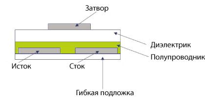
Schematic diagram of the OFET device
From device to separate OFET
Some types of polymers, for example, polyacetylene, have a "connected" system of atomic orbitals, which, when applied with some (frankly, not small) voltage, causes electrons to tunnel from one atom to another, jump, creating an electric current between the electrodes.
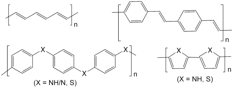
Examples of conductive polymers

Volt-ampere characteristic from the presentation Plastic Logic. Note: a change in the current by an order of magnitude requires a potential difference of 10 V, and by 3 orders of magnitude - 30 V.
To understand what kind of voltage for such jumps should be applied, take a look at the current-voltage characteristic taken from the English version of the PlasticLogic presentation. Changing the current by an order of magnitude requires 10 V, and three orders of magnitude more - about 30 V, which, to say the least, compared to silicon electronics (usually 5 V) is a bit too much, but you will have to sacrifice something.
Actually, it is (the development and production of TFT matrix displays) and forms the basis of the company's business, the trust of RosNano. Otherwise PlasticLogic readers are a hodgepodge. In addition, today, in addition to PlasticLogic, the ideology of plastic electronics is being promoted by LG , a certain organization TRADIM , they say that even for the iPhone was involved in this race, so the competition will be serious.
And the last. Fully organic microchips are a separate, big question that deserves a separate article. Maybe you,% username%, would like to devote a few days of painstaking search to it (I can even help;))?
But back to our ... experiments.
Experiment. Comparison of conventional E-Ink and display from PlasticLogic.
Let's not say where, but a small piece of PlasticLogic in my hands still turned out to be. And what else is needed for happiness?
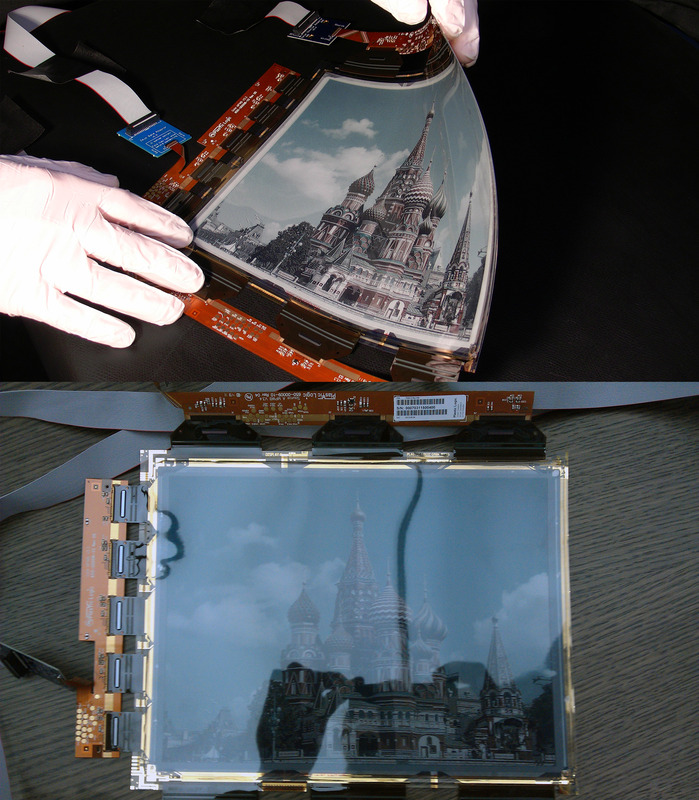
If you compare pixel sizes with the most common E-Ink display, which, by the way, was written not so long ago , it turns out that pixel sizes, or rather, thin-film transistors controlling these pixels, are quite comparable to each other, that is, the manufacturer simply optimized the structure of pixels under its technology, in some way without reducing their size (maybe the display is not high resolution caught?):
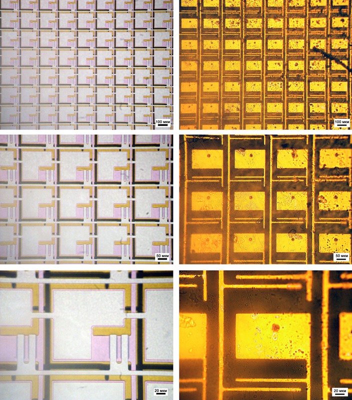
Comparison of E-Ink from PocketBook (left) and PlasticLogic control matrix (right)
For connoisseurs of the beautiful, there are two reports: what does E-Ink consist of and what do control transistors consist of . As for the first, E-Ink balls have a bit of aluminum, titanium, chromium and copper (that is, these are the elements that white and black dyes can consist of), and the film covering electronic paper of completely organic origin is really plastic electronics!
The second report is a bit more interesting, since it is dedicated to the story that silicon oxides are used as insulators in the transistors, and the contacts are made of gold, although representatives of PlasticLogic at the presentation said that there are no rare metals, which is why production cheapens ...
Who spoke on behalf of PlasticLogic?
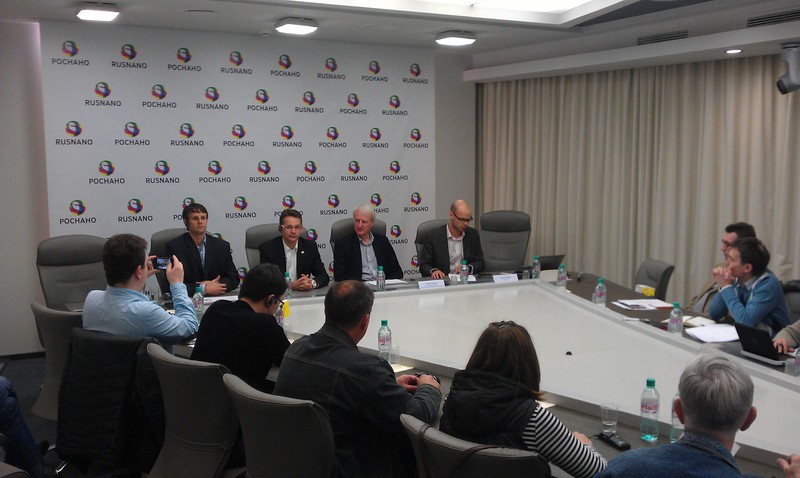
Peter Kitchin (second from right), vice president of the University of Cambridge Technology Center.
Peter Fisher (second from left), vice president of technology design
David Gammy, Senior Display Development Manager at Plastic Logic
Mike Banak (leftmost), senior research manager at Plastic Logic
More information about the biography of the speakers can be found here .
What was presented?
We talked about the history of the company, about people, technologies and trends ... Yes, that I'm talking all the time - see for yourself (presentation in English, in Russian, because of indecent quality, I refuse to post).
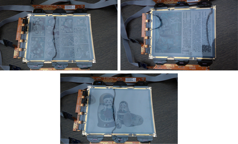
Of course, the most memorable were the color displays:
For comparison, a beautiful photo from the organizers (above) and how it actually looks like (below). There is a lack of “anti-glare”
And a little more pale color photos:
It is worth noting the insight of the organizers - portable microscopes:
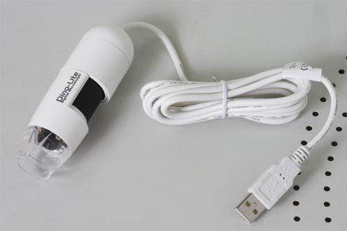
In my opinion, it was these cameras that were used to demonstrate the individual subpixels of the displays ( here is an overview of the microscopes)
With the help of these devices, we were able to look at color displays from a more familiar perspective, and also to compare high resolution and low resolution:
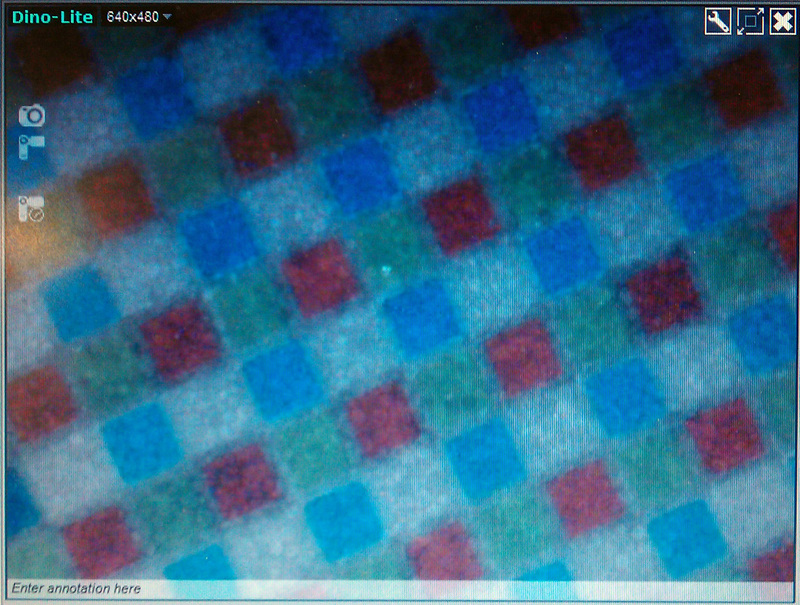
Just some pixels painted in the appropriate colors ...
Yes, exactly, so simple! Just put an additional layer of color filters and the display became color.
By the way, the creation of a color display required the development of E-Ink high definition. At the presentation there were displays with 225 PPI ( pixel per inch ). Since the formally declared color display resolution is 75 PPI, it turns out that representatives of PlasticLogic clearly clamped the display with 280 PPI somewhere (4 pixels on the color display form a pixel).
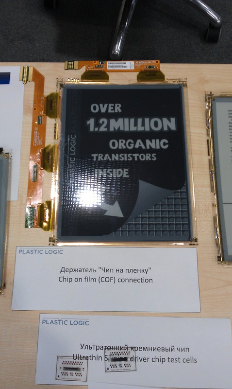
In addition to the transition to a pale color, a new trend was indicated: the landing of ultrathin silicon chips on a polymer substrate with wiring contacts. Please note that all presented photos contain similar silicon chips, maybe this driver?
PlasticLogic can make displays of completely different sizes, but for some reason prefer the A4 format to everyone else. For some reason it seems to me that this is their main competitive advantage (in particular, on the Russian market).
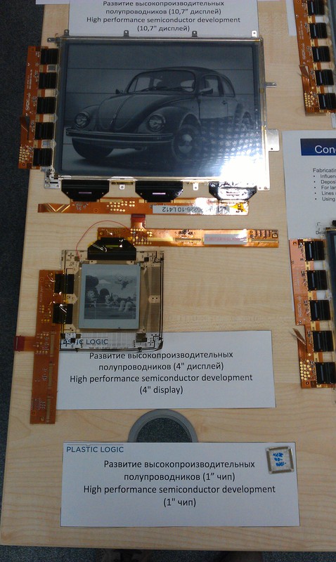
From small to big and back ...
Thinner, easier, faster and clearer - this is perhaps the slogan followed in PlasticLogic:
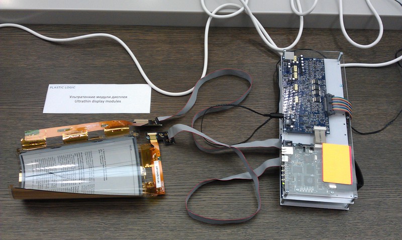
The display is really the thinnest and easiest, although during the presentation (2 hours) a lot of “dead” pixel lines appeared on it ...
This photo is worthy of "Mythbusters". I was all shocked to ask how many such displays were necessary so that the bullet would not pass - I could hardly resist:
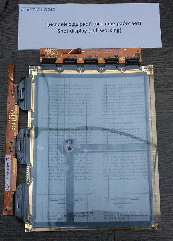
New market for PlasticLogic - body armor ... Joke, of course!
And another development of the company is a matrix with the possibility of backlight, i.e. the manufacturer, together with RosNano, really wants more and the market for flexible TVs, and possibly new projects:
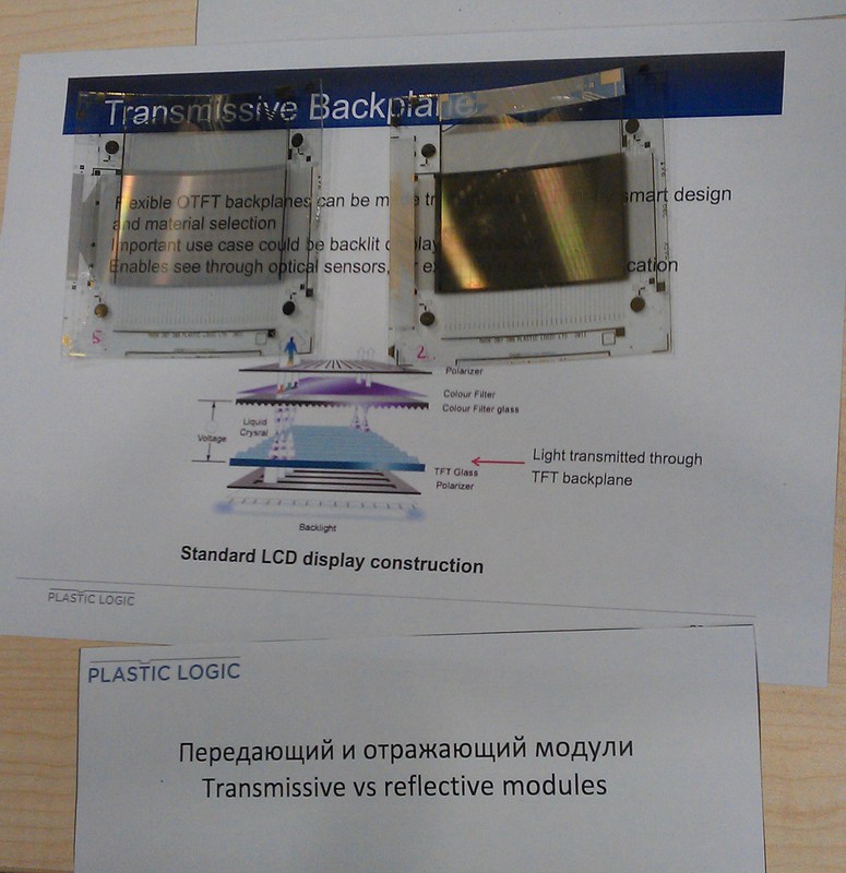
A good start for flexible TVs and monitors, and possibly a revolution in image projection systems
Moreover, there are even prototypes of flexible touch-displays, the use of which you can talk endlessly ... Yes, and in the above-mentioned presentation OFET applications are described in some detail - from RFID to TVs.
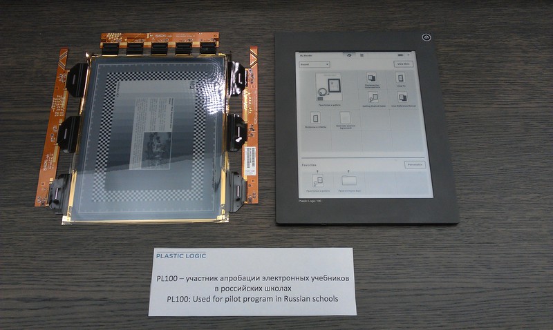
And finally, Chubais’s sensational school reader “unpacked” and “packed”. Well, let's see how it will be implemented. According to rumors, it is expected to sign a contract for the supply of such readers, then the plant in Dresden will work to its fullest.
And finally, two videos. One trend - cutting the display. I can not deny myself the pleasure to demonstrate it:
And a photo for memory:

It's alive! It's alive !!!
The second video clearly demonstrates that the films in the format of E-Ink be. I already vividly imagine textbooks on school chemistry or physics with revived Copernicus, Newton, telling about their laws, or atoms that either want or do not want to interact ... Already pulls back to school. Be sure to revive your favorite jokes:
findings
Conclusions that I made for myself after the presentation.
First , the transition to plastic electronics is inevitable: due to the rise in prices of rare metals used today in the manufacture of displays, and the desire for miniaturization. It is only a matter of time and technology development.
Secondly , RosNano, represented by PlasticLogic, joined the race very quickly. This is not a used line at the Sitronics factory with a morally obsolete 90-nm process technology. This is the leading edge of one of the directions of development of modern microelectronics. And I’m ready to give up and give all the key development opportunities to do in England, in the Cavendish Laboratory of Cambridge, the main thing is that then the production from Dresden moved to us (while we are talking about Zelenograd).
Thirdly , interesting solutions and development directions are shown: transparent matrixes (imagine a car in which the windshield is equipped with such a device and which displays a map, navigation, etc., or a 2/3 meter TV / projector), sensory panels (applications are virtually limitless), color and high-speed displays. All this can make another small but important revolution in IT and human-computer interfaces.
In the end I would like to add only one question: when will we learn to print the chips straight on our body? And it seems to me that very soon ...
PS : A few more interesting videos from the PlasticLogic channel on YouTube.
How does the factory in Dresden:
Backlit reader:
Bullying the display:
Tell me where to buy such a watch?
First , the full list of published articles on Habré:
Opening the Nvidia 8600M GT chip , a more detailed article is given here: Modern chips - a view from the inside
An inside look: CD and HDD
An inside look: LED bulbs
An inside look: the LED industry in Russia
An inside look: Flash and RAM
An inside view: the world around us
An inside look: LCD and E-Ink displays
An inside look: matrix digital cameras
An inside look: Plastic Logic
An inside look: RFID and other tags
An inside look: graduate school at EPFL. Part 1
An inside look: graduate school at EPFL. Part 2
An inside view: the world around us - 2
An inside view: the world around us - 3
An inside look: the world around us - 4
An inside look: 13 LED lamps and a bottle of rum. Part 1
An inside look: 13 LED lamps and a bottle of rum. Part 2
An inside look: 13 LED lamps and a bottle of rum. Part 3
An inside look: IKEA LED strikes back
An inside view: are Filament lamps good for you?
and 3DNews:
Microview: a comparison of modern smartphones displays
Secondly , in addition to the blog on HabraHabr , articles and videos can be read and viewed on Nanometer.ru , YouTube , and Dirty .
Thirdly , if you, dear reader, liked the article or you want to stimulate writing new ones, then act according to the following maxim: “pay what you want”
Yandex.Money 41001234893231
WebMoney (R296920395341 or Z333281944680)
Sometimes briefly, and sometimes not so much about the news of science and technology, you can read on my Telegram channel - welcome;)
Source: https://habr.com/ru/post/143949/
All Articles