An inside look: matrix digital cameras

Foreword
Two months ago, in an article about the comparison of LCD and E-Ink displays , I mentioned that one of the following reviews would be “opening” the matrix of a modern camera. And I hasten to fulfill this promise!
The front and back cameras of a smartphone by a well-known Korean manufacturer, courtesy of Vasily Stolyarov, were the first in the “collection” of photosensitive matrices. Then the DarkWood habrayuser , living not far from Moscow, sent me his old non-working Pentax camera (hereinafter I will not deliberately indicate the exact model of the device). The device was dead and it was a good reason to pass it into my caring hands, and not throw it out, as many do.
And as soon as I got ready to cut, I received another proposal from my practically classmate, Ilya. I could not refuse this offer. I was presented with a relatively modern Canon, which had problems with shooting images.
')
Thus, three candidates lay on the red-revolutionary May Day table: the OEM camera from the phone and the Pentax cameras (the oldest among all participants) and Canon (perhaps the youngest).
If someone else doesn’t know why we are here, then in the basement of this article there are links to previous “autopsies”. If someone forgot how a digital camera works or why a matrix is needed, then you are welcome to the Wiki or just watch this video from the Discovery channel:
Part of the theoretical. CCD and CMOS
Today, matrices made using CMOS technology (Complementary Metal-Oxide Semiconductor) have won more than 90% of the global market , and not so long ago the insanely popular CCD (Charge-Coupled Device) has already predicted a speedy decline.
The reasons for this are mass, this is not a complete list of the advantages of CMOS technology: firstly, low power consumption in a static state compared to CCD, secondly, CMOS immediately "produces" a digital signal that does not require additional conversion (more precisely, conversion occurs on each separate subpixel), unlike CCD, which is actually an analog device, and thirdly, low cost of production, especially for large matrix sizes.
You can briefly familiarize yourself with the principles of CMOS-matrix operation with the help of two videos from Canon:
But all of our patients (with the possible exception of the cell phone camera matrix) belong to the era when the world completely rules CCD, and CMOS only gained strength and sensitivity to subsequently take the leading position. Therefore, a few words, nevertheless, I will say about how the CCD matrix works. A more detailed description can always be found on the pages of the Wiki .
So, a photon from an object of shooting, passing through a Bayer filter , that is, a color filter like RGBG, or an RGBW filter and collecting microlens, falls on a photosensitive semiconductor material. Being absorbed, the photon generates an electric-hole pair, which in the cell under the action of an external electric field is “divided”, and the electron is “sent” to a piggy bank - a potential well, where it will expect to “read”.
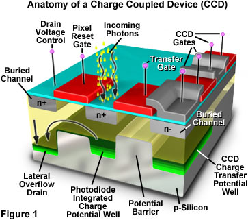
CCD matrix device diagram ( Source )
Reading in the CCD matrix happens “by the cell”, so to speak. Suppose we have an array of 5 by 5 pixels. First, we read the number of electrons, and simply the amount of electric current, from the first pixel. Then the special controller “shifts” all the cells by one, that is, the charge from the second cell flows into the first one. The value is read again, and so on, until all 5 cells have been read. Then another controller shifts the remaining “image” one line down and the process repeats until the currents in all 25 cells are measured. It may seem like a long process, but for 5 million pixels it takes only a fraction of a second.
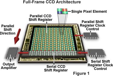
The process of reading images from a CCD matrix ( Source )
To make it completely clear, I suggest that you familiarize yourself with the following videos:
Part practical
Usually, people wearing snow-white gloves are engaged in beautiful analysis, they recently got to the cameras , but they say that you need to pay extra for the video assembly instructions by sending SMS to a short number. Further, a little more than completely clumsy methods will be applied, so I do not advise you to repeat this at home ...
How a cell phone was disassembled can always be viewed on the pages of the previous article , so I will not give these heartbreaking frames here again.
The aforementioned Pentax camera was provided by DarkWood's monsieur , who, it seems to me, must now bleed to his heart, and a man’s tears will roll down his cheek:
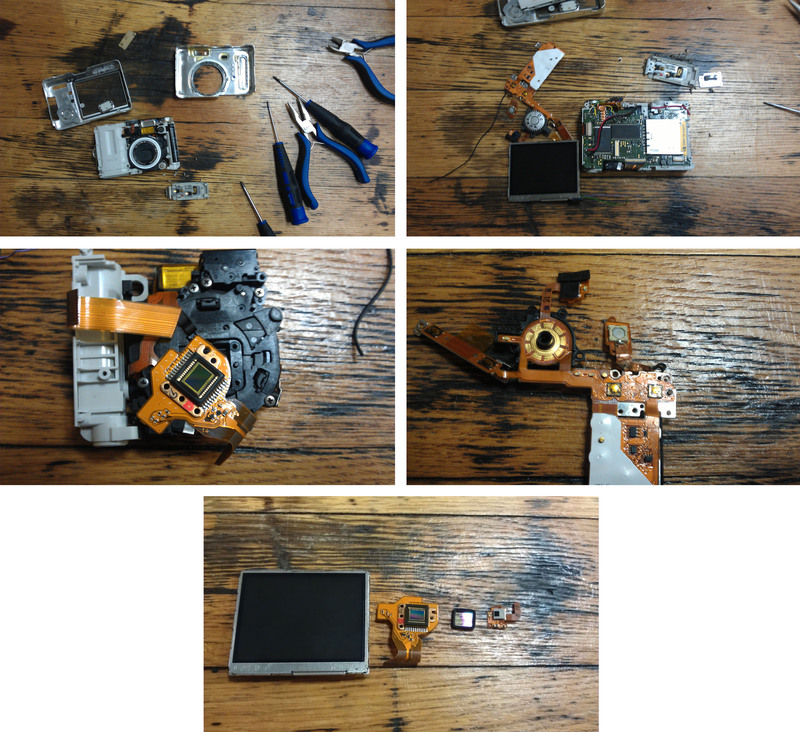
Pentax disassembly in photos
Of all the variety of details, we are only interested in the LCD display, which will be shown to schoolchildren coming to us, on the FNM, on an excursion, the CCD matrix itself, glass with something suspiciously reminiscent of a polarizer or filter and IR illumination (red light) for night shooting It is worth noting that the matrix is rigidly fixed on the camera body. Consequently, all the vibrations of your hands will easily be directly transmitted to the matrix itself, which, you see, does not contribute to high-quality photography. Apparently, DarkWood has reinforced nerves.
What, meanwhile, did not prevent him, "drown" your favorite camera. Remember, when in the summer you will recover in the warm countries of the sea and will try to take a picture of another roll of waves, that the camera is a device in which currents can lead to corrosion.

Traces of corrosion right on the train leading to the shutter button (unfortunately, not the only such place)
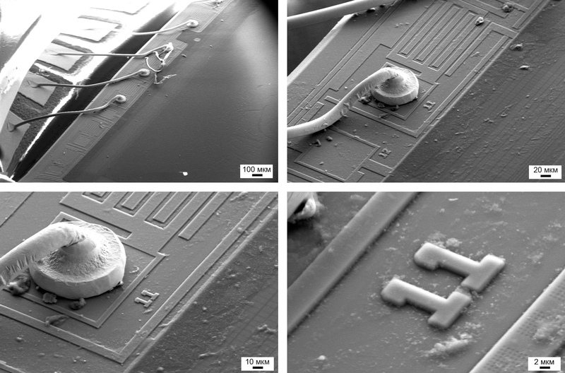
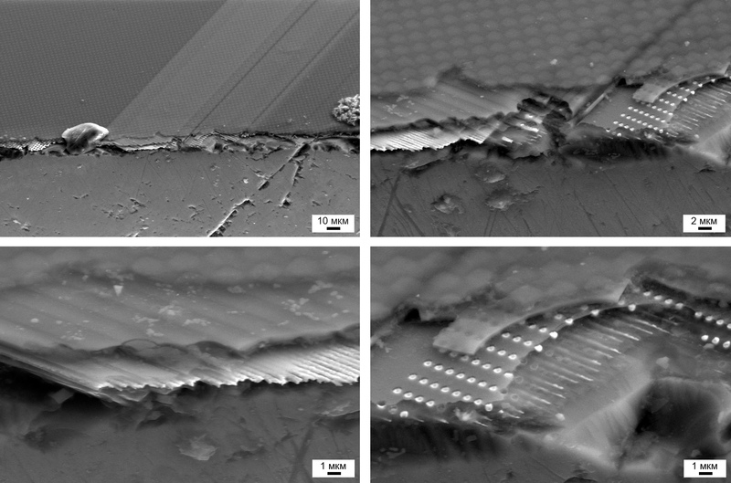
We immediately see that Canon is a bit more advanced, more modern model than Pentax. For example, the matrix is spring-loaded (small springs are clearly distinguishable in the lower left image). Such a passive image stabilization system contributes to obtaining better and clearer pictures, if, of course, you are not a neurasthenic in an advanced stage!

Canon's "Internals"
By the way, in the photo on the right below you can clearly see the huge condenser responsible for the flash, because of the problems with which I once had to write off my Canon digital soap box.
Mobile phone camera
We begin our research with a mobile phone camera, which is not much time and words will be devoted in this article due to the fact that the matrix itself has completely microscopic dimensions and it is difficult to work with it (saw, grind).
As it is not difficult to notice, on optical micrographs below the matrix at the edge has two zones: lighter and darker. I hope that everyone has already guessed: there are no diodes under the bright side, it is applied just like that, with a margin in order to maximally close the thin mental organization of the matrix ...
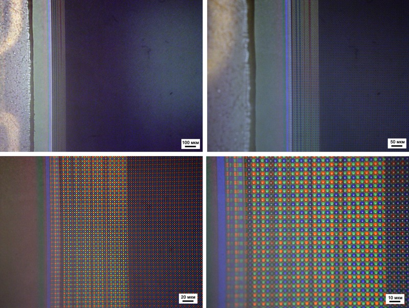
We will cover everything with a margin - we do not mind
Micrographs taken with an optical microscope are significantly different from those produced by an electron microscope. For example, how about the “quadrature of a sphere”?
The fact is that we do not see any transparent layers on optics (yes, even if they are just less noticeable), while electron microscopy is primarily a method of surface analysis, that is, it may well be that the round color filters are covered from above square "caps". In this case, the dimensions of such a cubo-spherical sub-pixel are about 2.5 micrometers.
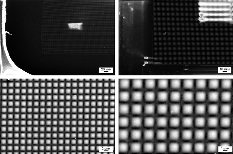
Here it is, the quadrature of the sphere ... by the way, in a vacuum ...
Camera matrix Pentax
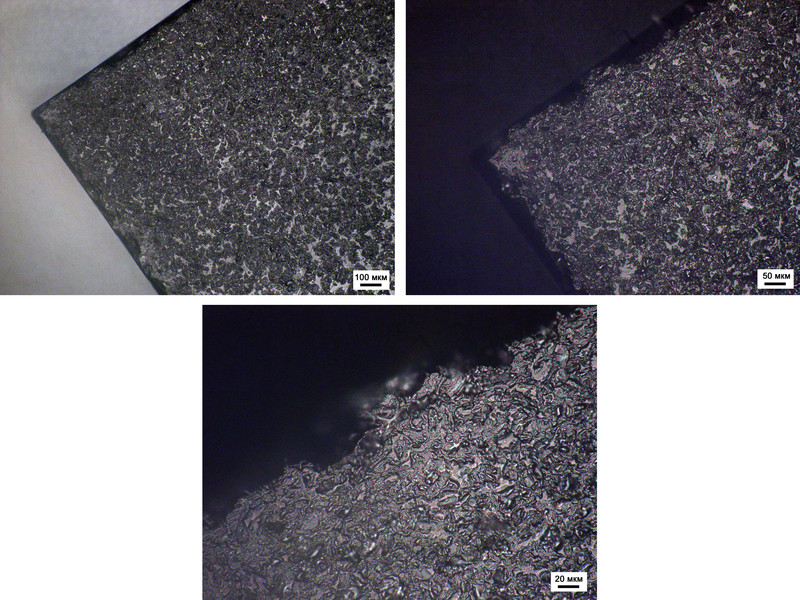
We will begin the study of the CCD matrix of the Pentax camera with optical microphotographs. To my deep regret, because of the steric difficulties, as the chemists say, the microscope sample in the system could not be removed at high magnifications and the individual subpixels were examined.

Something is written, it is interesting, but is it possible to see the names of the little Chinese kids somewhere?
Each landing pad under the contacts is numbered, but not the same contact wire is connected to each.
And this is how we will soon learn to count - with the help of nanotechnology, naturally ...
A clear boundary between the matrix itself and the “strapping”
And the next micrograph is worthy of a textbook on electron microscopy. Do you know why an electron microscope is not a measure? Yes, that's why: due to the local accumulation of charge, it seems that spherical objects suddenly became ellipsoids:

But we know that these are spheres ...
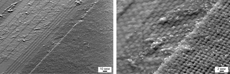
Next, take a look at what is around the photosensitive matrix. Since I am not an expert in the field of creating electronic circuits, I’m even afraid to suggest why we need all these complex constructions and the “intricacies” of conductors, maybe someone will be ready to explain the purpose of the details and components below (in the comments, of course same)?
Unshakable posts, survivors of cutting and polishing ...
In these layers, you can get confused, and break the leg and leg
This issue of “A View from the Inside” is a landmark, after several years of “ordeals” we, at last, have installed a new microanalysis system, so in some cases, I can not only bring beautiful pictures, but also explain what chemical elements are seen.
And here's the most interesting - the matrix in all its glory. Under the mesh, in the cells of which the microspheres-lenses are located, one can see individual photosensitive elements (or their remains, or, more precisely, difficult). Below, when discussing the Canon matrix, I will explain in detail the “cross-section” matrix device. In the meantime, we turn to the data of local chemical analysis. It turns out that the grid consists of tungsten, and the microspheres, apparently, it is silicon dioxide, which is “covered” from above with some kind of polymeric material. More detailed analysis can be found here .
The matrix in all its sophisticated beauty
Returning to the first SEM image in this chapter, I would like to note that the contact pads are made of pure gold (oh yes!), However, the conductors inside the sensor appear to consist of aluminum, on which copper is deposited with the thinnest layer instrument sensitivity. Detailed information is presented here .
Matrix camera Canon
As usual, we continue our immersion in micro and nanoworlds with optical microscopy. As in the case of Pentax, the matrix from the Canon camera could not be removed at high magnification due to geometric inconsistencies. However, from the micrographs obtained, it is possible to estimate the size of an individual subpixel — about 1.5 μm, which is much smaller than the matrix of a mobile phone.
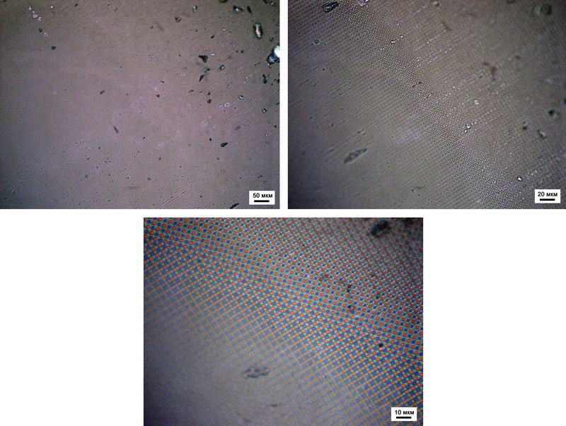
Canon optical micrographs
By the way, one of the culprits of the impossibility to shoot on an optical microscope at high magnifications is a “cover glass” covering the matrix and its “stuffing”:

Good shot: pass behind the glass
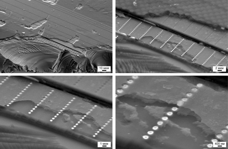
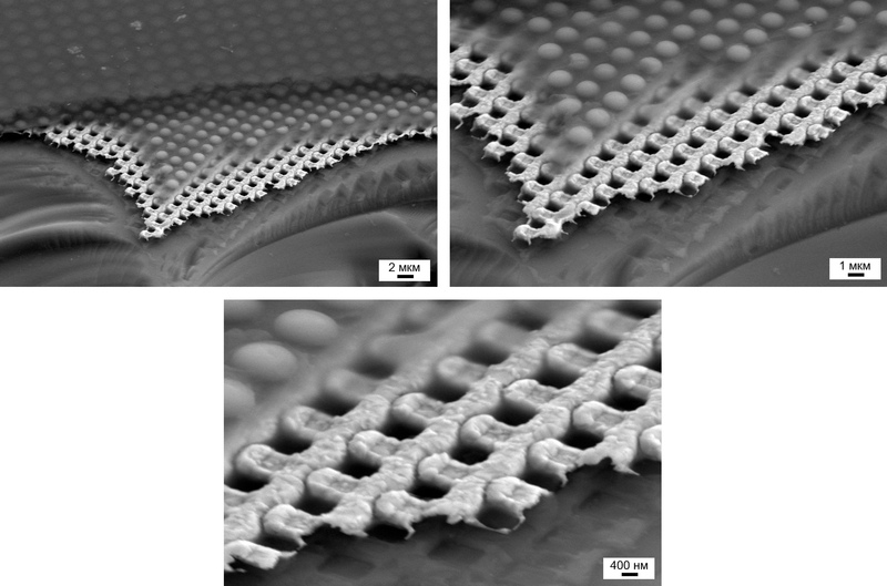
Of course, always the most interesting thing is hiding on chips, where a collapsing strictly ordered world gives a crack, which allows you to look into the most sacramental corners of the device:
A little later, we will return to the yellowish-orange areas of this photo ...
Already familiar to us columns of completely incomprehensible purpose:
How Persistent Tin Soldiers
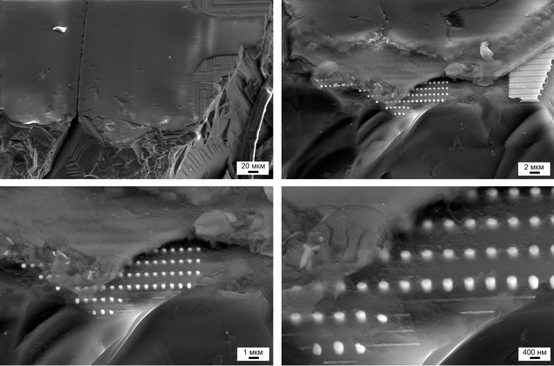
Now consider in more detail the device CCD-matrix. On top of the CCD-matrix is covered with something resembling a polymer layer (1), which protects the photosensitive elements from an aggressive external environment. Under it are microlenses with dye (2 and 3). But since electron microscopy does not allow to obtain color images, it is not possible to say exactly whether a large or small sphere is colored. Silicon dioxide microlenses (the most likely material for their manufacture) are fixed in the cells of a tungsten grid (4), under which the photosensitive elements (5) hide. And, of course, this whole structure rests on a substrate of the purest silicon!
Given that the matrix is additionally protected by a “cover” glass, then the photocells are better protected than the President of the Russian Federation in his limousine (unless, of course, corrected for the scale factor).
Microanalysis data can be downloaded here .

The device matrix points. Description in the text
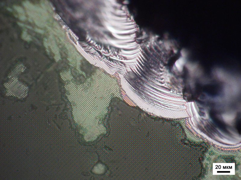
But that's not all. We still have a glass window covering the matrix, which, it seems, is a polarizer. It is somewhat rough around the edges, but almost perfectly smooth over the rest of the surface area. It seems that optical microscopy does not give any results: glass, like glass.
Glass with suspicion of polarizer: nothing unusual
And only with the help of electron microscopy it is possible to see the chemical contrast on the image and the striped structure. The thickness of such a “film” is only 2.5 micrometers, while the dimensions of the individual layers are 180 and 100 nm, respectively, for darker and lighter ones. Based on the microanalysis data ( here ), I would venture to suggest that darker areas are enriched with titanium, and light areas - with aluminum. In my opinion, this is amazing!

It turns out that inside the camera has its own striped life!
Afterword
Such a world of the passing century of CCD-matrices appeared before us today.
Thanks to everyone (Vasily for the phone, Ilya and DarkWood for the cameras), who made a contribution to the creation of this article. You - well done, that supported in this difficult endeavor!
And the apotheosis of this article, but rather its apophigous:

Rest in peace until we come up with a new application.
Bonus 1. What does a green dust storm look like in Moscow?
I first wanted to post a separate post, but decided not to litter the space. Just a few days ago, a yellow-green cloud covered Moscow , many had already begun to prepare for the arrival of the apocalypse, but nothing happened ... What in reality was the reason for such a strange coloring?
The climate has lately tinkled up on this planet: it will leave the New Year without snow, it will fill up with snow to the very top, then spring will look like winter, then suddenly summer will come. Flowers, trees and vegetation are less adapted to this kind of perturbations, so 1.5 months of spring, shrinking in 1 week, forced the plants to reconsider their plans for reproduction ...
In the morning, sitting at my desk, I found a layer of dust on it, and after wiping it with a napkin, I realized that I should study this dust properly. No sooner said than done!
But for all I have two news: good and bad.
The good news is that the color of the yellow-green cloud was really due to a large amount of pollen (I counted at least three types):

The composition of the Moscow storm: pollen ... bottom right pollen on the surface of the plant
The bad news is that we breathe too, and every day, and not during plant breeding periods (micro- and nanoparticles, which not every filter will catch):

The composition of the Moscow storm: not very pleasant dust and dirt
Bonus 2. Guess what is it?
PS Recently, a large number of posts devoted to the subject of copyright and "pay what you want" began to appear on HabraHabr. For example, they collect donations in favor of ReactOS or for publishing / writing books . I thought and decided to “get involved” in this, too, so it's up to you, dear readers:
Yandex.Money 41001234893231
WebMoney (R296920395341 or Z333281944680)
For a week, we managed to collect about 2,500 rubles - THANKS to all who responded and made their own contribution !!!;)
PPS By the way, I unexpectedly discovered that some of my works under the cutting of certain items move people to their own discoveries .
First , the full list of published articles on Habré:
Opening the Nvidia 8600M GT chip , a more detailed article is given here: Modern chips - a view from the inside
An inside look: CD and HDD
An inside look: LED bulbs
An inside look: the LED industry in Russia
An inside look: Flash and RAM
An inside view: the world around us
An inside look: LCD and E-Ink displays
An inside look: matrix digital cameras
An inside look: Plastic Logic
An inside look: RFID and other tags
An inside look: graduate school at EPFL. Part 1
An inside look: graduate school at EPFL. Part 2
An inside view: the world around us - 2
An inside view: the world around us - 3
An inside look: the world around us - 4
An inside look: 13 LED lamps and a bottle of rum. Part 1
An inside look: 13 LED lamps and a bottle of rum. Part 2
An inside look: 13 LED lamps and a bottle of rum. Part 3
An inside look: IKEA LED strikes back
An inside view: are Filament lamps good for you?
and 3DNews:
Microview: a comparison of modern smartphones displays
Secondly , in addition to the blog on HabraHabr , articles and videos can be read and viewed on Nanometer.ru , YouTube , and Dirty .
Thirdly , if you, dear reader, liked the article or you want to stimulate writing new ones, then act according to the following maxim: “pay what you want”
Yandex.Money 41001234893231
WebMoney (R296920395341 or Z333281944680)
Sometimes briefly, and sometimes not so much about the news of science and technology, you can read on my Telegram channel - welcome;)
Source: https://habr.com/ru/post/143169/
All Articles