Holey Optochip light chipset
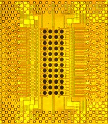 Since 2008, IBM researchers have been developing optical chipsets, whose main difference from traditional ones is ultra-high data transfer rates (up to 8Tbps / 1TBps). The innovative chip design, using 48 small round holes in a standard CMOS board, allows light (laser beam) to transmit information at an average speed of almost terabits per second.
The new chip is much faster and uses less energy than modern optics, which are used to transfer all the information inside the computer and networks. “Holey Optochip”, which is the name of the novelty, can already be used (and is used) inside supercomputer clusters today.
Optical chips that drive data with light, instead of electrons, are still used only for internal networks of supercomputer points, like the Power 775 and Blue Gene. Every year, such technologies are becoming more and more popular: “Ten years ago, the supercomputer №1 did not have a single application of optical technologies or anything like that, but now we see their use for connecting computing clusters inside and outside the racks,” says IBM Optical Links Group Clint Show (Clint Schow).
Thus, the performance of the entire cluster is approaching the notorious processor power, speeding up the entire network operation. Moreover, the goal is to create a connection of several processors within the system, not memory accesses, namely the communication of computational cores in a large parallel system.
')
The new chip uses 4.7 watts transmitting a trillion bits per second. The size of the novelty is 5.2 mm by 5.8 mm. Compact enough?

Since the chip itself is built on an unmodified silicon plate like CMOS, it can quickly be on the wide market — you do not need to build new lines and conveyors using any technologies to produce it: “This chip has a standard electronic circuit, supporting light connection. Only drivers are needed to control the laser beam and receivers that convert the photocurrent from the detector into a workable electrical signal. ”
As for lasers that transmit information from one chip to another, IBM uses the usual 850-meter lasers (VCSEL) attached to one side of the chip and photodiodes mounted on the back side. Optical access is formed precisely by a two-sided structure, which is quite compact due to the use of holes, and not “attachments”.
"Holes are needed anyway, because the silicon substance from which the chip is made cannot transmit light - and it must go right through," explains Shaw. In the rack where the chips are placed, they are installed exactly one above the other, and the laser beam hits the back of each chip (where the detector is located), and the board sends its already modified light signal to the next chips in its row.
A standard optical chip today has 12 channels (each hole is a channel - the connection between the receiver and the transmitter), each of which transmits 10 Gigabits per second. In Holey Optochip, there are 48 such channels and each works at 20 Gigabits per second, reaching a total speed of 960 Gigabits. On Thursday, at the Optical Fiber Communication Conference, which is held in Los Angeles, IBM will present its development to the general public as the first optical chip that can drive one trillion bits of data from device to device.
As Clint Shaw says: “This is a breakthrough, since we have four times more channels operating at double speed, with energy consumption almost four times less than usual”. When recalculating the effectiveness of watts / bits, it turns out that this is one of the most energy-efficient microcircuits on the planet.
However, the speed of one channel remains more or less standard, especially considering the fact that IBM used standard components for the construction of the board and the company noted that increasing the speed of data transmission in each individual hole is a near goal: “There are already developments that will allow speeds of 25 gigabits per second per channel. " The most magnificent is the architecture, which allows you to adjust the flux density, power and speed depending on conditions and goals.

"You can make the board work very quickly if you are indifferent to energy costs, or you can be very energy efficient if you don't care about speed," says Shaw. As always, the most difficult thing is keeping the golden mean. Actually, even the current chip is not the first (as I hinted at the very beginning) an experienced copy of an optical electronic device - in 2010, the first prototype of such a chip showed a speed of 300 gigabits per second, and in 2007 - 160 gigabits per second work supercomputer Deep Blue.
As for the mass production of these chips, there are some minor difficulties - IBM will not independently start their production, preferring to give a license to this to companies with great potential in the field of iron design. Although Clint Shaw looks at this very positively, saying that most likely in the next year or two everyone will have the opportunity to purchase such a chip for themselves (it is not clear why, hardly every second collects a computing cluster at home) at a price between $ 100 and $ 200 .
“Our development is only a small product of one group within IBM Research, which is trying to bring communication technologies in the field of big data, analytic applications and everything else, where for normal operation the throughput must be very high. Our mission is to prototype technologies, demonstrate their performance. We do not know who will make a specific commercial decision, the main thing is that we can use it in our systems. ”
Source: https://habr.com/ru/post/139817/
All Articles