STM32F1хх - we continue treatment for arduine dependence with the help of LCD
Good afternoon, dear habrovchane. In my last article, I reviewed the use of the excellent STM32F1xx microcontrollers using the example of servo control. In this article, we turn to a more interesting question - the management of color graphic LCD-display. In addition to the standard work with the display, I will try to highlight the issues of using the features of STM32F microcontrollers to effectively address this issue. So, let's begin.
A small addition to the introduction - this article was started more than six months ago, but then I had to stop (first the defense of my graduation project, then a lot of urgent projects at work), and the time was found only now. Therefore, it turned out now, of course, not quite the same as I imagined at the beginning, some of the code and graphic material would be lost - but still, I tried to finish it, and I hope that it will be interesting for you.
First of all, about the gland. The core of the system, as well as last time, will be the STM32VLDISCOVERY debugging board, which can be purchased for 300r. We will assemble the circuit on a breadboard to solder less. However, unlike last time, we still have to solder, and quite a specific one - we will have to solder to a flexible-rigid printed circuit board at the back of the display (to put it simply, to a film with contacts). But more about that later. The 3.3V power supply is on the debug board, so all we need in addition is the display itself and a 10-20 volt power supply for its illumination.
It is time to consider the part for which everything, in fact, was started - the display.
In fact, the options available to the developer at home, quite a lot.
At the time of writing this article, I considered displays from mobile phones to be the most affordable option, since they are relatively easy to buy, many are controlled by SPI and are quite cheap. Actually, this article is devoted to one of such displays.
However, after I spent some time on e-bay, I came to the conclusion that the best option is, after all, the purchase of a separate display for your needs.
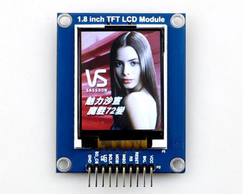
First, you can find pretty cheap models, such as, for example, this display:

1-8-TFT-Color-LCD-Display-Module-SPI-interface
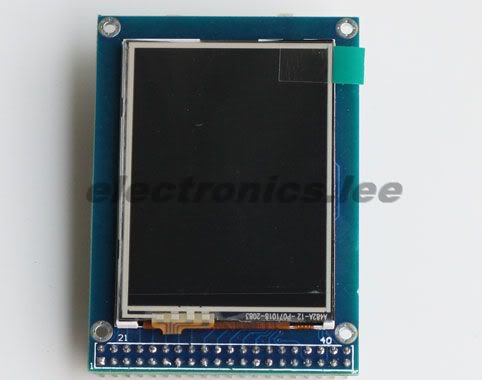
Secondly, if you pay a little more, you can get a complete display module and don’t waste time soldering uncomfortable connectors:
1-8-TFT-LCD-module-TF-Card-socket-break-out-arduino
')
Thirdly, some display modules are altogether beyond all praise -
2-4inch-TFT-LCD-module-touch-panel-SD-card-cage
For 18 bucks, we get a fully finished display module, which includes a 320x240 display with a controller, which has full documentation (note that the display controllers from many mobile phones are very difficult to find documentation), a resistive touchscreen with a controller (that is, it is already connected , you can immediately request the coordinates by SPI), a convenient connector, and - as a bonus appendage - a slot for micro-SD.
Also on board is a boost converter to power the backlight.
Therefore, at the moment, I, of course, consider displays with e-bay the most convenient and correct option.
Finally, the last option that I would like to point out, these are such amusing devices:
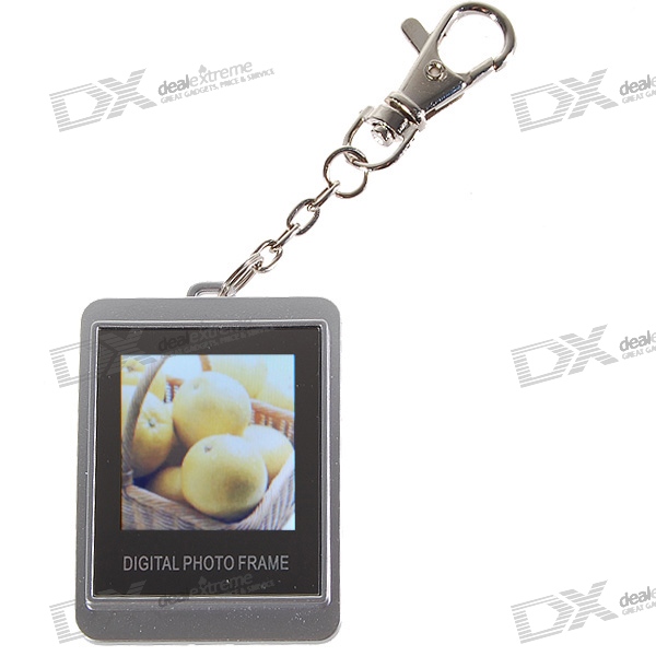
1-5-lcd-rechargeable-digital-usb-photo-frame-keychain
This miracle of Chinese technology is a miniature digital photo frame. As it turned out, several foreign enthusiasts were already digging in its depths, and found out that they are being built on the ST2203U 6502-compatible microcontroller, whose firmware is fixed during production, so we are not interested. On the other hand, in less than 200p we get a 128x128 STN LCD display (most of them are built on the PCF8833 controller), a flash memory chip, a lithium-ion battery with a charge controller circuit and a handy case for its device.
And yet, let’s dwell on the first option, that is, the display from a mobile phone.
According to information taken from the Internet, from small color LCD displays, displays from Nokia HZ and Siemens S (K) 65 are popular. There is quite a lot of information on the first display, but it is inferior to displays from Siemens in image quality, resolution, and most importantly - in response time, which makes it almost unsuitable for playing animation. And you and I are not interested in displaying static pictures, right? The second display, according to data from the Internet, provides us with a resolution of 132 x 176 pixels and a response time sufficient to display the animation. However, unfortunately, I had no opportunity to compare these two displays - because I hung around the old Siemens SK65, the choice was clearly made in favor of it.
The first rake lies in wait for us when buying the display itself. The fact is that Siemens installs in its S65 displays on the controllers of three different manufacturers, LS020xxx, LPH88xxxx, L2F50xxx.


About the third, I have not heard anything at all, on the second there is an official datasheet, but it seems that this controller is much less common.
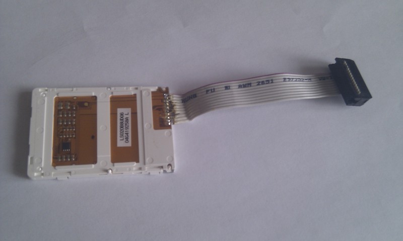
But first, the LS020xxx is the controller that most often stands on mobiles, and my SK65 was no exception.
It would seem that everything is fine, but here lies one unpleasant fact: there is no datasheet on the controller. Thus, it is necessary to develop without an official document, in which commands and registers would be described. But not everything is so bad - the craftsmen conducted a reverse engineering session and determined the basics of interaction with the display, and there is a lot of information about it on the Internet.
Consider the display in more detail.

The first thing that catches your eye is a very convenient contact pads, which are much easier to solder to than the smaller connectors on most displays. True, they are located on a flex-rigid printed circuit board, which, if carelessly applied, can be melted with a soldering iron, so that when soldering we set the temperature of the soldering iron to a smaller one.
Total display has 10 contacts:
The LED + and LED_GND contacts are powered by the display backlight, which can be from 10 to 20 volts. This power is supplied to 3 LEDs, the current through them is regulated by the controller schematics, so that one or two 9V batteries without current-limiting resistors can be connected to them fearlessly. I connected two series-connected, slightly hooked, crowns, receiving a voltage of about 17V.
The 1V8, 2V9 and GND pins provide power to the display circuits. What is interesting, in many wiring diagrams, you can see the pin 1V8 is not connected at all. In all other schemes, the pins 1V8 and 2V9 are connected together and connected to the source 3.3V. This connection turned out to be quite workable, so we will do it.
Pins CS, DAT, CLK show us a trivial SPI interface without a return wire. This fact can not but rejoice, because even on AVRs, there is a hardware SPI controller, and STMs are rich to the periphery of this kind - there are two of these controllers in the low-end models, 4 are high in the older ones, so one of the SPIs can be selected entirely for communication with the display.
The RS and RESET pins are two additional control signals for the display. The first, being in the active level (log 0), indicates that we are transmitting commands to the display, and in the inactive (log 1) data. RESET, as the name implies, is designed to reset the controller.
Now we need to connect the display to our debug board using the layout. For this, I selected a cable with a 10-pin IDC connector.
I realized my tactical blunder when the cable was already soldered - the fact is that the horizontal sockets on the breadboard are interconnected, so the rows of the connector are shorted. Anyway, I didn’t have another connector anyway, so I had to make amendments in the form of “legs” of wire - because The layout consists of three independent sections, by connecting a connector on the border of sections, it was possible to avoid a short circuit.
Those who will repeat my experiments still advise you to take a single-row 10-pin connector, problems will be less. After the cable is crimped, it should be soldered to the contacts of the display - I remind you that the film on which the contacts are located does not like long-term exposure to high temperature, so we try to solder quickly and clearly.
After soldering, place the connector on the breadboard and begin to connect with jumpers to the controller. The power supply pins of the backlight are immediately diverted to hell, we plug the connector in there from the crown and forget about them. Whoever has a 10-20V power supply is even better, you do not have to constantly disconnect the batteries in order to save energy.
Next, the SPI interface is connected. The debug board in the prototype was installed only by hanging the horizontal pins (for the reason for the jumper already described), which fortunately were few. However, among them was the SPI2 interface, so that only the first one remained at our disposal. However, it should not upset us greatly, because we are not going to connect anything to it yet. Therefore we connect CLK with pin PA7, DAT - with pin PA5. We will pull the CS with handles in accordance with the logic of operation, as well as the RS with the RESET - therefore, we will output these three signals where it is convenient for us. I chose pins PA2, PA3, PA4. You end up with something like this:

By the way, a small offtopic: after I connected everything, I issued a test 10 KHz meander to one of the pins. And this is what the oscilloscope showed:
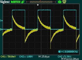
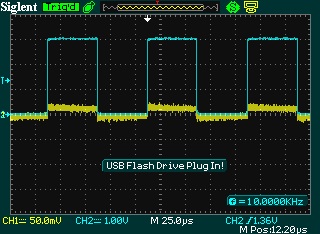
Channel 2, marked in blue, is connected to the pin itself. But channel 1 (yellow) is connected to the adjacent output. See these beautiful exhibitors with an amplitude of almost 100mV? All these jumpers on the breadboard give a rather weak capacitive coupling between the pins. Which is typical, if the debug board is pulled out of the layout, the effect is practically absent:
Therefore, when designing a device, be careful: the layout makes its own specifics, which must be considered. High-frequency circuits to collect on it is almost impossible.
After connecting the display, we take out the multimeter and carefully check the assembly, ringing all the signals, so as not to sin on the firmware when you have the postings.
If everything is connected correctly, run Cale and proceed to the next part.
As I already mentioned, I returned to writing the article many months after, in fact, experimenting with the display, so part of the code was lost. But I tried to restore important points from memory. However, the interaction with the display is very trivial and should not cause difficulties.
So, at the moment we need to have a display fully connected to the breadboard and running Cale with the project created.
We begin with a simple display of images. Since our task now is to deal with the display, we will not philosophize slyly and screw up the download from the cards, reading the file systems, etc. - just place the image as raw 16-bit RGB values in the controller's flash memory. To do this, I recommend to jot down a program in a convenient programming language that will translate a standard bmp file into a record like
Since the resolution of our display is 132 x 176 pixels, each of which takes 2 bytes, the full picture will take up 46,464 bytes in memory, that is, a little more than 45 KB.
Fortunately, 500 KB of flash STMki allow us to save the image in its raw form, and not even one.
Now go to the display programming. Most of all it looks like black magic, because we don’t have datasheets for the controller, but there are instructions from those who reverse that immediately give a “spell” as a sequence of bytes, without explaining why it is. If you are not satisfied with this approach, then the best solution would be to purchase any of the displays I mentioned from the e-bay, to which a complete set of documentation goes.
So, spells.
The display is initialized with the following sequence (very sensitive to pauses!):
After that, a multi-colored garbage should appear on the display, meaning that the initialization was successful.
So, we will try to implement it all, incidentally remembering how to work with the periphery in STMke.
I decided to try bit-banding at the same time, for which I immediately announced three pointers:
For those who do not remember about this wonderful technique, bit-banding is a very useful feature, representing the mapping of each bit of the IO-registers and RAM in the dvd somewhere in the STMki address space. Since the address space is 32-bit, that is, 4 gigabytes, and actually much less involved, the developers decided to spend a few meters to link bits from the IO or RAM (bit-band alias region) with dvords in the bit-band region .
It works simply - let's say we want to manage the pin of CS, which corresponds to PA2. The level of the signal on it is controlled by bit number 2 of the GPIOA-> ODR register.
Let's use the formula from datasheet:
bit_word_addr = bit_band_base + (byte_offset x 32) + (bit_number × 4)
bit_word_addr is the address of the bit band to be calculated.
bit_band_base for our processor, according to the datasheet, is declared in the header as
byte_offset - offset to the desired register, in this case, to GPIOA-> ODR, from the beginning of the bit-band alias region.
Since the address of GPIOA-> ODR is 0x4001080, and the beginning of the peripheral bit-band alias of the region is declared as
That offset will be 0x4001080-0x40000000 = 0x1080C
And finally, the number of the bit of interest to us is 2. Combining it all together we get
* CS = 0x42000000 + (0x1080C) * 32 + 2 * 4 = 0x42000000 + 210180 + 8 = 0x42210188
Now, by writing a nonzero value at this address, we set the bit associated with this memory cell to 1, and writing zero to 0.
Three blocks of bytes have already been announced, we will initialize the periphery:
Everything is simple - we set Reset, CS, RS to exit under the control of our program,
CLK and MOSI - output controlled by the periphery, that is, in this case, the controller SPI.
SPI is tuned to the Fclk / 8 frequency and data sending by 16-bit words instead of bytes.
You should also describe the functions of delay and synchronous sending by SPI, which, due to their triviality, I will not give here, except for the prototypes:
Their implementation is extremely simple - the delay is implemented by a normal cycle, synchronous sending via SPI - sending a byte to the SPI data register (SPI1-> DR = Data;) and waiting in the cycle until the SPI_SR_BSY flag disappears from the SPI1-> SR status .
Further we carry out our magic sequence:
Now it's time to learn new spells. So:
The command {0xEF90, 0x05OR, 0x06XX, 0x07YY} - displays graphic information on the screen, where the OR byte indicates the orientation of the screen when outputting and can be equal to 0x04 in the case of horizontal and 0x00 in the case of vertical - pixels will be filled in this direction. Bytes XX and YY indicate the position of the lower left corner of the rectangle. The upper right corner will always be equal to the pixel (175, 131).
Then you should submit bytes of graphic information in the format on which the display was initialized. In this case - 16-bit Word of the form 5-6-5 (RGB)
To display information in a limited area, the command is used in a slightly modified form:
{0xEF90, 0x05OR, 0x08X1,0x09X2,0x0AY1,0x0BY2}, where X1, Y1 are the coordinates of the lower left corner of the output area, X2, Y2 are the coordinates of the upper right corner.
Thus, filling the entire screen with black will look like this:
Well, now we will finally display our picture!
If everything is done correctly, then we should get the following result:

Mirrored marine as it tells us: remember the order of the output pixels!
Finishing work with the display is recommended not by simply turning off the power, but by the following sequence of commands:
On this, in principle, it would be possible to finish, but in fact, ahead of us the most interesting is waiting for us!
So, we brought to the screen a picture from memory. This is already a good achievement and a wide field for activity, but ... We could do the same thing easily on the notorious Arduin. And our goal is to recover from arduino dependence and understand which tasks are best solved by other methods. Let's think: what is the current implementation limiting us to?
The answer is obvious - if we want to render the animation, then most of the time we will be spinning in a cycle of displaying graphical information. Since the screen resolution is 132x176 pixels, each of which is described by two bytes, we need to display 371,712 bits on the SPI bus. Each bit is output with a frequency of eight times less than the clock, that is, we need to spend 2,973,696 cycles to output one frame. Having a 75 MHz STMK on hand is perhaps not so critical - albeit unpleasant, but for 16 MHz AVRki is a disaster at all.
But fortunately, in the STM architecture there is a block that in such situations makes our life look like a fairy tale. This is a direct memory access unit, that is, a DMA.
It allows data transfer without the use of the controller core between the following points:
Quite a word, let's actually see what it gives us!
First, add the necessary code to the initialization of the peripherals:
Here we set the address where the data will be written (it is equal to the SPI data register address), set the number of 16-bit words for transmission to be 1560 (my frames are 30x52 pixels in size), the average transmission priority is
the size of the receiver and the source - in this case, both of them are 16 bits, the direction of transmission (from memory to the periphery), set the pointer autoincrement to the memory, and enable DMA.
After that we should prepare several frames in the same format as the const uint16_t Picture [] described earlier.
For this, I prepared 12 headers frame01.h ... frame12.h, and combined the data from them into
We also introduce a frame counter variable.
It remains quite a bit - in the initialization we tune the system timer to the frame rate we need,
It remains to describe the timer interrupt handler:
Here we calculate the number of our next frame, after which we disable the DMA transmission for a while. This is necessary to transfer the display commands to the graphics output.
In this case, small pictures are displayed, not full screen, because simply not enough memory controller. If you screw here reading from any SD-card, then it is quite possible to twist the full-screen video.
After the commands are transmitted, we set up the address of the source of the graphics — one of the frames, the pointers to which are stored in Video [], set the size of the transmitted block and enable DMA.
Everything! Now our program spends no more than a few tens of cycles on the output of graphics every 50 ms, the same ones that go on processing a timer interrupt - after the interrupt is processed, DMA starts sending data to the SPI register without our participation! Thus, we can safely do our work in the main cycle, prepare the next frame, or short-cut any objects without worrying about the output of graphics.
If everything is done correctly, we get the following:
What have we achieved?
First of all, we learned to work with such interesting peripherals as a color graphic display. This in itself is not bad and can be useful in projects.
But the main thing is that we have learned how to use the DMA block, which opens up the widest possibilities, compared to the soft data transfer on controllers that do not have such a block.
As for the displays, I would like to add the following: on e-bay I found a debug board, which I would call without question an excellent and necessary developer tool on STM32. It is sold here: Mini-STM32
For 45 bucks we get an incredibly convenient and powerful tool, which includes the STM32F103VET microcontroller, with hardware USB, a static memory controller, which at times facilitates work with the display and the hardware controller of SD cards. The display itself, with a resolution of 320x240 and a resistive touchscreen installed on it, a touchscreen controller, a boost converter for powering the backlight. All necessary binding for USB. RS-232 with converter. And the battery that feeds the controller's back-up registers.
Also, on additional request, for $ 28 in the order will add a convenient programmer, clone J-LINK, which, according to my feelings, is much more stable than the one that is built into the debug for 300r.
In general, I highly recommend to anyone who is going to engage in STMs to purchase a kit from this debug board and programmer. I will write subsequent articles using the Mini-STM32 as the main tool.
Since at the moment I am working with very interesting radio modules, the next article will most likely be about them.
Understanding the display, I used the following materials:
http://www.juras-projects.org/eng/lcd.php
http://avrhobby.ru/index.php?option=com_content&view=article&id=71:-rgb-1&catid=42:rgb-&Itemid=71
A small addition to the introduction - this article was started more than six months ago, but then I had to stop (first the defense of my graduation project, then a lot of urgent projects at work), and the time was found only now. Therefore, it turned out now, of course, not quite the same as I imagined at the beginning, some of the code and graphic material would be lost - but still, I tried to finish it, and I hope that it will be interesting for you.
Iron
First of all, about the gland. The core of the system, as well as last time, will be the STM32VLDISCOVERY debugging board, which can be purchased for 300r. We will assemble the circuit on a breadboard to solder less. However, unlike last time, we still have to solder, and quite a specific one - we will have to solder to a flexible-rigid printed circuit board at the back of the display (to put it simply, to a film with contacts). But more about that later. The 3.3V power supply is on the debug board, so all we need in addition is the display itself and a 10-20 volt power supply for its illumination.
It is time to consider the part for which everything, in fact, was started - the display.
In fact, the options available to the developer at home, quite a lot.
At the time of writing this article, I considered displays from mobile phones to be the most affordable option, since they are relatively easy to buy, many are controlled by SPI and are quite cheap. Actually, this article is devoted to one of such displays.
However, after I spent some time on e-bay, I came to the conclusion that the best option is, after all, the purchase of a separate display for your needs.
First, you can find pretty cheap models, such as, for example, this display:
1-8-TFT-Color-LCD-Display-Module-SPI-interface
Secondly, if you pay a little more, you can get a complete display module and don’t waste time soldering uncomfortable connectors:
1-8-TFT-LCD-module-TF-Card-socket-break-out-arduino
')
Thirdly, some display modules are altogether beyond all praise -
2-4inch-TFT-LCD-module-touch-panel-SD-card-cage
For 18 bucks, we get a fully finished display module, which includes a 320x240 display with a controller, which has full documentation (note that the display controllers from many mobile phones are very difficult to find documentation), a resistive touchscreen with a controller (that is, it is already connected , you can immediately request the coordinates by SPI), a convenient connector, and - as a bonus appendage - a slot for micro-SD.
Also on board is a boost converter to power the backlight.
Therefore, at the moment, I, of course, consider displays with e-bay the most convenient and correct option.
Finally, the last option that I would like to point out, these are such amusing devices:
1-5-lcd-rechargeable-digital-usb-photo-frame-keychain
This miracle of Chinese technology is a miniature digital photo frame. As it turned out, several foreign enthusiasts were already digging in its depths, and found out that they are being built on the ST2203U 6502-compatible microcontroller, whose firmware is fixed during production, so we are not interested. On the other hand, in less than 200p we get a 128x128 STN LCD display (most of them are built on the PCF8833 controller), a flash memory chip, a lithium-ion battery with a charge controller circuit and a handy case for its device.
And yet, let’s dwell on the first option, that is, the display from a mobile phone.
According to information taken from the Internet, from small color LCD displays, displays from Nokia HZ and Siemens S (K) 65 are popular. There is quite a lot of information on the first display, but it is inferior to displays from Siemens in image quality, resolution, and most importantly - in response time, which makes it almost unsuitable for playing animation. And you and I are not interested in displaying static pictures, right? The second display, according to data from the Internet, provides us with a resolution of 132 x 176 pixels and a response time sufficient to display the animation. However, unfortunately, I had no opportunity to compare these two displays - because I hung around the old Siemens SK65, the choice was clearly made in favor of it.
The first rake lies in wait for us when buying the display itself. The fact is that Siemens installs in its S65 displays on the controllers of three different manufacturers, LS020xxx, LPH88xxxx, L2F50xxx.
About the third, I have not heard anything at all, on the second there is an official datasheet, but it seems that this controller is much less common.
But first, the LS020xxx is the controller that most often stands on mobiles, and my SK65 was no exception.
It would seem that everything is fine, but here lies one unpleasant fact: there is no datasheet on the controller. Thus, it is necessary to develop without an official document, in which commands and registers would be described. But not everything is so bad - the craftsmen conducted a reverse engineering session and determined the basics of interaction with the display, and there is a lot of information about it on the Internet.
Consider the display in more detail.
Display LS020xxx
The first thing that catches your eye is a very convenient contact pads, which are much easier to solder to than the smaller connectors on most displays. True, they are located on a flex-rigid printed circuit board, which, if carelessly applied, can be melted with a soldering iron, so that when soldering we set the temperature of the soldering iron to a smaller one.
Total display has 10 contacts:
- RS command / data switch signal
- RESET - display reset signal
- CS - SPI device select signal
- CLK - SPI Clock
- DAT - MOSI SPI signal
- 2.9V and 1.8V - display power
- LED +, LED_GND - power and ground circuit lighting
- GND is the display ground.
The LED + and LED_GND contacts are powered by the display backlight, which can be from 10 to 20 volts. This power is supplied to 3 LEDs, the current through them is regulated by the controller schematics, so that one or two 9V batteries without current-limiting resistors can be connected to them fearlessly. I connected two series-connected, slightly hooked, crowns, receiving a voltage of about 17V.
The 1V8, 2V9 and GND pins provide power to the display circuits. What is interesting, in many wiring diagrams, you can see the pin 1V8 is not connected at all. In all other schemes, the pins 1V8 and 2V9 are connected together and connected to the source 3.3V. This connection turned out to be quite workable, so we will do it.
Pins CS, DAT, CLK show us a trivial SPI interface without a return wire. This fact can not but rejoice, because even on AVRs, there is a hardware SPI controller, and STMs are rich to the periphery of this kind - there are two of these controllers in the low-end models, 4 are high in the older ones, so one of the SPIs can be selected entirely for communication with the display.
The RS and RESET pins are two additional control signals for the display. The first, being in the active level (log 0), indicates that we are transmitting commands to the display, and in the inactive (log 1) data. RESET, as the name implies, is designed to reset the controller.
Now we need to connect the display to our debug board using the layout. For this, I selected a cable with a 10-pin IDC connector.
I realized my tactical blunder when the cable was already soldered - the fact is that the horizontal sockets on the breadboard are interconnected, so the rows of the connector are shorted. Anyway, I didn’t have another connector anyway, so I had to make amendments in the form of “legs” of wire - because The layout consists of three independent sections, by connecting a connector on the border of sections, it was possible to avoid a short circuit.
Those who will repeat my experiments still advise you to take a single-row 10-pin connector, problems will be less. After the cable is crimped, it should be soldered to the contacts of the display - I remind you that the film on which the contacts are located does not like long-term exposure to high temperature, so we try to solder quickly and clearly.
After soldering, place the connector on the breadboard and begin to connect with jumpers to the controller. The power supply pins of the backlight are immediately diverted to hell, we plug the connector in there from the crown and forget about them. Whoever has a 10-20V power supply is even better, you do not have to constantly disconnect the batteries in order to save energy.
Next, the SPI interface is connected. The debug board in the prototype was installed only by hanging the horizontal pins (for the reason for the jumper already described), which fortunately were few. However, among them was the SPI2 interface, so that only the first one remained at our disposal. However, it should not upset us greatly, because we are not going to connect anything to it yet. Therefore we connect CLK with pin PA7, DAT - with pin PA5. We will pull the CS with handles in accordance with the logic of operation, as well as the RS with the RESET - therefore, we will output these three signals where it is convenient for us. I chose pins PA2, PA3, PA4. You end up with something like this:
By the way, a small offtopic: after I connected everything, I issued a test 10 KHz meander to one of the pins. And this is what the oscilloscope showed:
Channel 2, marked in blue, is connected to the pin itself. But channel 1 (yellow) is connected to the adjacent output. See these beautiful exhibitors with an amplitude of almost 100mV? All these jumpers on the breadboard give a rather weak capacitive coupling between the pins. Which is typical, if the debug board is pulled out of the layout, the effect is practically absent:
Therefore, when designing a device, be careful: the layout makes its own specifics, which must be considered. High-frequency circuits to collect on it is almost impossible.
After connecting the display, we take out the multimeter and carefully check the assembly, ringing all the signals, so as not to sin on the firmware when you have the postings.
If everything is connected correctly, run Cale and proceed to the next part.
Code
As I already mentioned, I returned to writing the article many months after, in fact, experimenting with the display, so part of the code was lost. But I tried to restore important points from memory. However, the interaction with the display is very trivial and should not cause difficulties.
So, at the moment we need to have a display fully connected to the breadboard and running Cale with the project created.
We begin with a simple display of images. Since our task now is to deal with the display, we will not philosophize slyly and screw up the download from the cards, reading the file systems, etc. - just place the image as raw 16-bit RGB values in the controller's flash memory. To do this, I recommend to jot down a program in a convenient programming language that will translate a standard bmp file into a record like
const uint16_t Picture[] = {0x0000, 0x0000, …, 0x0000}; Since the resolution of our display is 132 x 176 pixels, each of which takes 2 bytes, the full picture will take up 46,464 bytes in memory, that is, a little more than 45 KB.
Fortunately, 500 KB of flash STMki allow us to save the image in its raw form, and not even one.
Now go to the display programming. Most of all it looks like black magic, because we don’t have datasheets for the controller, but there are instructions from those who reverse that immediately give a “spell” as a sequence of bytes, without explaining why it is. If you are not satisfied with this approach, then the best solution would be to purchase any of the displays I mentioned from the e-bay, to which a complete set of documentation goes.
So, spells.
The display is initialized with the following sequence (very sensitive to pauses!):
- Log level 0 to the RESET line and hold it for about 5 ms
- We give the first spell to the display, which is such a block of bytes:
uint16_t Init1[12]={0xFDFD,0xFDFD,0xEF00,0xEE04, 0x1B04,0xFEFE,0xFEFE,0xEF90, 0x4A04,0x7F3F,0xEE04,0x4306}
Replacing Init1 [9] = 0x7F3F with 0x7F1F, we can initialize the display in 256 color mode - but since 16-bit color is still more interesting, let's focus on the original version.
After this block bytes must wait 7 ms. - We issue a block byte
uint16_t Init2[20]={0xEF90,0x0983,0x0800,0x0BAF,0x0A00, 0x0500,0x0600,0x0700,0xEF00,0xEE0C, 0xEF90,0x0080,0xEFB0,0x4902,0xEF00, 0x7F01,0xE181,0xE202,0xE276,0xE183}
And wait 50 ms - Kastuem last spell in the form of two bytes
uint16_t Init3[2]={0x8001}
After that, a multi-colored garbage should appear on the display, meaning that the initialization was successful.
So, we will try to implement it all, incidentally remembering how to work with the periphery in STMke.
I decided to try bit-banding at the same time, for which I immediately announced three pointers:
uint32_t *Reset = (uint32_t*)0x42210184, *CS = (uint32_t*)0x42210188, *RS = (uint32_t*)0x4221018C; For those who do not remember about this wonderful technique, bit-banding is a very useful feature, representing the mapping of each bit of the IO-registers and RAM in the dvd somewhere in the STMki address space. Since the address space is 32-bit, that is, 4 gigabytes, and actually much less involved, the developers decided to spend a few meters to link bits from the IO or RAM (bit-band alias region) with dvords in the bit-band region .
It works simply - let's say we want to manage the pin of CS, which corresponds to PA2. The level of the signal on it is controlled by bit number 2 of the GPIOA-> ODR register.
Let's use the formula from datasheet:
bit_word_addr = bit_band_base + (byte_offset x 32) + (bit_number × 4)
bit_word_addr is the address of the bit band to be calculated.
bit_band_base for our processor, according to the datasheet, is declared in the header as
#define PERIPH_BB_BASE ((uint32_t)0x42000000) byte_offset - offset to the desired register, in this case, to GPIOA-> ODR, from the beginning of the bit-band alias region.
Since the address of GPIOA-> ODR is 0x4001080, and the beginning of the peripheral bit-band alias of the region is declared as
#define PERIPH_BASE ((uint32_t)0x40000000) That offset will be 0x4001080-0x40000000 = 0x1080C
And finally, the number of the bit of interest to us is 2. Combining it all together we get
* CS = 0x42000000 + (0x1080C) * 32 + 2 * 4 = 0x42000000 + 210180 + 8 = 0x42210188
Now, by writing a nonzero value at this address, we set the bit associated with this memory cell to 1, and writing zero to 0.
Three blocks of bytes have already been announced, we will initialize the periphery:
RCC->APB2ENR |= RCC_APB2ENR_IOPAEN; RCC->APB2ENR |= RCC_APB2ENR_SPI1EN; GPIOA->CRL |=GPIO_CRL_MODE1; GPIOA->CRL &=~GPIO_CRL_CNF1; GPIOA->CRL |=GPIO_CRL_MODE2; GPIOA->CRL &=~GPIO_CRL_CNF2; GPIOA->CRL |=GPIO_CRL_MODE3; GPIOA->CRL &=~GPIO_CRL_CNF3; GPIOA->CRL |=GPIO_CRL_MODE5; GPIOA->CRL &=~GPIO_CRL_CNF5; GPIOA->CRL |=GPIO_CRL_CNF5_1; *Reset=1; *CS=1; *RS=1; GPIOA->CRL |=GPIO_CRL_MODE7; GPIOA->CRL &=~GPIO_CRL_CNF7_0; GPIOA->CRL |=GPIO_CRL_CNF7_1; SPI1->CR1 &= ~SPI_CR1_BR_2; SPI1->CR1 |= SPI_CR1_DFF; SPI1->CR1 |= SPI_CR1_MSTR|SPI_CR1_SPE; Everything is simple - we set Reset, CS, RS to exit under the control of our program,
CLK and MOSI - output controlled by the periphery, that is, in this case, the controller SPI.
SPI is tuned to the Fclk / 8 frequency and data sending by 16-bit words instead of bytes.
You should also describe the functions of delay and synchronous sending by SPI, which, due to their triviality, I will not give here, except for the prototypes:
__INLINE void Delay_ms(uint32_t us) __INLINE void SendSPI(uint16_t Data) Their implementation is extremely simple - the delay is implemented by a normal cycle, synchronous sending via SPI - sending a byte to the SPI data register (SPI1-> DR = Data;) and waiting in the cycle until the SPI_SR_BSY flag disappears from the SPI1-> SR status .
Further we carry out our magic sequence:
*Reset=0; *CS=0; Delay_ms(5); *Reset=1; Delay_ms(50); for(i=0;i<12;i++) SendSPI(Init1[i]); Delay_ms(7); for(i=0;i<20;i++) SendSPI(Init2[i]); Delay_ms(50); for(i=0;i<2;i++) SendSPI(Init3[i]); Delay_ms(5); Now it's time to learn new spells. So:
The command {0xEF90, 0x05OR, 0x06XX, 0x07YY} - displays graphic information on the screen, where the OR byte indicates the orientation of the screen when outputting and can be equal to 0x04 in the case of horizontal and 0x00 in the case of vertical - pixels will be filled in this direction. Bytes XX and YY indicate the position of the lower left corner of the rectangle. The upper right corner will always be equal to the pixel (175, 131).
Then you should submit bytes of graphic information in the format on which the display was initialized. In this case - 16-bit Word of the form 5-6-5 (RGB)
To display information in a limited area, the command is used in a slightly modified form:
{0xEF90, 0x05OR, 0x08X1,0x09X2,0x0AY1,0x0BY2}, where X1, Y1 are the coordinates of the lower left corner of the output area, X2, Y2 are the coordinates of the upper right corner.
Thus, filling the entire screen with black will look like this:
SendSPI(0xEF90); SendSPI(0x0504); SendSPI(0x0600); SendSPI(0x0700); *RS=0; for(i=0;i<132*176;i++) SendSPI(0x0000); *RS=1; *CS=1; Well, now we will finally display our picture!
SendSPI(0xEF90); SendSPI(0x0504); SendSPI(0x0600); SendSPI(0x0700); *RS=0; for(i=0;i<132*176;i++) SendSPI(Picture[i]); *RS=1; *CS=1; If everything is done correctly, then we should get the following result:
Mirrored marine as it tells us: remember the order of the output pixels!
Finishing work with the display is recommended not by simply turning off the power, but by the following sequence of commands:
uint16_t Power[26]={0xEF00,0x7E04,0xEFB0,0x5A48,0xEF00,0x7F01,0xEFB0,0x64FF,0x6500,0xEF00,0x7F01,0xE262,0xE202,0xEFB0,0xBC02,0xEF00,0x7F01,0xE200,0x8000,0xE204,0xE200,0xE100,0xEFB0,0xBC00,0xEF00,0x7F01}; *RS=1; for(i=0;i<26;i++) SendSPI(Power[i]); *CS=1; On this, in principle, it would be possible to finish, but in fact, ahead of us the most interesting is waiting for us!
Using the features of the architecture STM32F1xx to optimize the display on the screen
So, we brought to the screen a picture from memory. This is already a good achievement and a wide field for activity, but ... We could do the same thing easily on the notorious Arduin. And our goal is to recover from arduino dependence and understand which tasks are best solved by other methods. Let's think: what is the current implementation limiting us to?
The answer is obvious - if we want to render the animation, then most of the time we will be spinning in a cycle of displaying graphical information. Since the screen resolution is 132x176 pixels, each of which is described by two bytes, we need to display 371,712 bits on the SPI bus. Each bit is output with a frequency of eight times less than the clock, that is, we need to spend 2,973,696 cycles to output one frame. Having a 75 MHz STMK on hand is perhaps not so critical - albeit unpleasant, but for 16 MHz AVRki is a disaster at all.
But fortunately, in the STM architecture there is a block that in such situations makes our life look like a fairy tale. This is a direct memory access unit, that is, a DMA.
It allows data transfer without the use of the controller core between the following points:
- Memory memory
- Memory Peripherals
- Peripherals-Memory.
Quite a word, let's actually see what it gives us!
First, add the necessary code to the initialization of the peripherals:
DMA1_Channel3->CPAR = (uint32_t)(&SPI1->DR); DMA1_Channel3->CNDTR = 1560; DMA1_Channel3->CCR |= DMA_CCR3_PL_0; DMA1_Channel3->CCR |= DMA_CCR3_PSIZE_0; DMA1_Channel3->CCR |= DMA_CCR3_MSIZE_0; DMA1_Channel3->CCR |= DMA_CCR3_DIR; DMA1_Channel3->CCR |= DMA_CCR3_MINC; DMA1_Channel3->CCR |= DMA_CCR3_EN; Here we set the address where the data will be written (it is equal to the SPI data register address), set the number of 16-bit words for transmission to be 1560 (my frames are 30x52 pixels in size), the average transmission priority is
the size of the receiver and the source - in this case, both of them are 16 bits, the direction of transmission (from memory to the periphery), set the pointer autoincrement to the memory, and enable DMA.
After that we should prepare several frames in the same format as the const uint16_t Picture [] described earlier.
For this, I prepared 12 headers frame01.h ... frame12.h, and combined the data from them into
const uint16_t* Video[]={frame1,frame2,frame3,frame4,frame5,frame6,frame7,frame8,frame9,frame10,frame11,frame12}; We also introduce a frame counter variable.
uint8_t FrameCnt=0; It remains quite a bit - in the initialization we tune the system timer to the frame rate we need,
SysTick_Config(SystemCoreClock/50000); It remains to describe the timer interrupt handler:
void SysTick_Handler() { *CS=0; FrameCnt++; if(FrameCnt>11) FrameCnt=0; SPI1->CR2 &= ~SPI_CR2_TXDMAEN; DMA1_Channel3->CCR &=~DMA_CCR3_EN; *RS=1; *CS=0; SendSPI(0xEF90); SendSPI(0x0504); SendSPI(0x0A00+70); SendSPI(0x0800+50); SendSPI(0x0B1D+70); SendSPI(0x0933+50); *RS=0; DMA1_Channel3->CMAR = (uint32_t)Video[FrameCnt]; DMA1_Channel3->CNDTR = 1560; DMA1_Channel3->CCR |= DMA_CCR3_EN; SPI1->CR2 |= SPI_CR2_TXDMAEN; } Here we calculate the number of our next frame, after which we disable the DMA transmission for a while. This is necessary to transfer the display commands to the graphics output.
In this case, small pictures are displayed, not full screen, because simply not enough memory controller. If you screw here reading from any SD-card, then it is quite possible to twist the full-screen video.
After the commands are transmitted, we set up the address of the source of the graphics — one of the frames, the pointers to which are stored in Video [], set the size of the transmitted block and enable DMA.
Everything! Now our program spends no more than a few tens of cycles on the output of graphics every 50 ms, the same ones that go on processing a timer interrupt - after the interrupt is processed, DMA starts sending data to the SPI register without our participation! Thus, we can safely do our work in the main cycle, prepare the next frame, or short-cut any objects without worrying about the output of graphics.
If everything is done correctly, we get the following:
Conclusion
What have we achieved?
First of all, we learned to work with such interesting peripherals as a color graphic display. This in itself is not bad and can be useful in projects.
But the main thing is that we have learned how to use the DMA block, which opens up the widest possibilities, compared to the soft data transfer on controllers that do not have such a block.
As for the displays, I would like to add the following: on e-bay I found a debug board, which I would call without question an excellent and necessary developer tool on STM32. It is sold here: Mini-STM32
For 45 bucks we get an incredibly convenient and powerful tool, which includes the STM32F103VET microcontroller, with hardware USB, a static memory controller, which at times facilitates work with the display and the hardware controller of SD cards. The display itself, with a resolution of 320x240 and a resistive touchscreen installed on it, a touchscreen controller, a boost converter for powering the backlight. All necessary binding for USB. RS-232 with converter. And the battery that feeds the controller's back-up registers.
Also, on additional request, for $ 28 in the order will add a convenient programmer, clone J-LINK, which, according to my feelings, is much more stable than the one that is built into the debug for 300r.
In general, I highly recommend to anyone who is going to engage in STMs to purchase a kit from this debug board and programmer. I will write subsequent articles using the Mini-STM32 as the main tool.
Since at the moment I am working with very interesting radio modules, the next article will most likely be about them.
Links
Understanding the display, I used the following materials:
http://www.juras-projects.org/eng/lcd.php
http://avrhobby.ru/index.php?option=com_content&view=article&id=71:-rgb-1&catid=42:rgb-&Itemid=71
Source: https://habr.com/ru/post/139384/
All Articles